A silicon nitride Si3N4 PCB is the toughest ceramic circuit board available for high-power electronics, with a fracture toughness of 6–7 MPa·√m — roughly 5× that of alumina and 3× that of aluminum nitride. That mechanical advantage makes the silicon nitride Si3N4 PCB the substrate of choice wherever thermal cycling, vibration, or mechanical shock would crack a more brittle ceramic. Its thermal conductivity of 70–90 W/mK sits between alumina (24–28 W/mK) and AlN (170–200 W/mK), which is adequate for most high-power applications when paired with a properly designed copper layer via active metal brazing (AMB).
Key Takeaways
- Si3N4 substrates achieve fracture toughness of 6–7 MPa·√m (per Kyocera SN series datasheet), enabling survival through >3,000 thermal cycles from −55 °C to +250 °C.
- Thermal conductivity ranges from 70–90 W/mK at 25 °C depending on grade, measured per ASTM E1461 (laser flash method).
- The primary metallization process for silicon nitride Si3N4 PCB substrates is AMB (active metal brazing); DBC is possible but less common due to bonding challenges with Si3N4 surfaces.
- Si3N4 substrates cost roughly 3–5× more than equivalent AlN substrates and 8–15× more than 96% alumina, so they are justified only when reliability under thermal cycling is the dominant requirement.
- Typical applications include EV traction inverters (SiC/GaN modules), railway power converters, aerospace power electronics, and high-reliability industrial drives.
What Is a Silicon Nitride Si3N4 PCB?
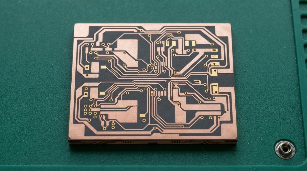
A silicon nitride Si3N4 PCB is a circuit board built on a Si3N4 ceramic substrate, typically 0.32 mm thick, with copper traces bonded to one or both sides using AMB. Si3N4 is a covalently bonded ceramic with an interlocking grain microstructure that gives it far higher flexural strength (600–900 MPa per ASTM C1161) than any other substrate ceramic. The material’s coefficient of thermal expansion (CTE) is approximately 2.6–3.0 ppm/°C at 25–400 °C, which creates a moderate mismatch with copper (17 ppm/°C) and silicon (2.6 ppm/°C) or SiC (4.0 ppm/°C) die.
The critical distinction from alumina or AlN substrates is that Si3N4 absorbs the stress from CTE mismatch without cracking. During thermal cycling, microcracks that would propagate through Al2O3 or AlN are arrested by the elongated β-Si3N4 grain structure. This is why Si3N4 dominates in power modules rated for automotive-grade reliability, where qualification standards like AQG 324 require thousands of thermal-shock cycles. For a broader comparison of substrate ceramics, see the ceramic substrate material selection guide.
Si3N4 PCB Material Properties Compared to Other Ceramic Substrates
The table below puts the silicon nitride Si3N4 PCB substrate in context against the three other ceramics commonly used for circuit boards. All values are typical ranges for commercially available grades.
| Parameter | Si3N4 | AlN | Al2O3 96% | Al2O3 99.6% | Unit | Condition |
|---|---|---|---|---|---|---|
| Thermal conductivity | 70–90 | 170–200 | 24–28 | 30–35 | W/mK | 25 °C, ASTM E1461 |
| Flexural strength | 600–900 | 300–400 | 300–380 | 380–450 | MPa | 3-pt bend, ASTM C1161 |
| Fracture toughness (KIC) | 6–7 | 2.5–3.0 | 3.5–4.0 | 3.8–4.5 | MPa·√m | SEVNB, 25 °C |
| CTE | 2.6–3.0 | 4.5–5.0 | 7.0–7.4 | 7.2–7.6 | ppm/°C | 25–400 °C |
| Dielectric strength | 15–18 | 14–17 | 10–15 | 12–16 | kV/mm | 25 °C, IEC 60243 |
| Typical substrate thickness | 0.25–0.64 | 0.25–1.0 | 0.25–2.0 | 0.25–1.0 | mm | — |
| Relative cost (per cm²) | 8–15× | 3–5× | 1× (baseline) | 1.5–2× | — | vs. 96% Al2O3 |
Typical values for commercially available material, for comparison only. Confirm against the datasheet for your specific grade.
The standout metric is fracture toughness. At 6–7 MPa·√m, Si3N4 is in a different class from every other substrate ceramic. This translates directly into thermal-cycle life. An AMB-bonded Si3N4 substrate routinely survives >3,000 cycles at ΔT = 250 °C (−40 °C to +250 °C), while an equivalent AlN substrate may crack between 500 and 1,500 cycles under the same profile, per published data from Kyocera and CeramTec. For a deep dive into Si3N4 material grades and measurement methods, see the Si3N4 properties and datasheet page.
Why Si3N4 Survives Thermal Cycling Better Than AlN or Alumina
The mechanism is grain bridging. During sintering, Si3N4 develops elongated β-phase grains that interlock like a three-dimensional mesh. When a crack initiates at the copper-ceramic interface under thermal stress, these elongated grains bridge the crack faces and absorb energy through friction and pull-out. The crack slows and stops. In equiaxed-grain ceramics like alumina, cracks propagate along grain boundaries with minimal resistance.
This matters most in power modules where thick copper layers (0.3–0.8 mm) are bonded to the substrate. Thicker copper improves current-carrying capacity and thermal spreading, but it also increases the stress at the ceramic interface during each temperature swing. Si3N4 is the only substrate ceramic that reliably supports 0.8 mm copper on both sides through automotive-grade thermal cycling per AQG 324.
Worked Example: Thermal-Cycle Stress Estimate
Consider a substrate with 0.3 mm copper on a 0.32 mm ceramic, cycled between −40 °C and +175 °C (ΔT = 215 °C). The approximate maximum interfacial shear stress τ can be estimated from:
τ ≈ ECu × Δα × ΔT × (tCu / L)
Where ECu ≈ 120 GPa, Δα (CTE mismatch, Cu vs. Si3N4) ≈ 14.5 ppm/°C, ΔT = 215 °C, tCu = 0.3 mm, and L = half the copper pad length (say 10 mm).
τ ≈ 120 × 10³ × 14.5 × 10⁻⁶ × 215 × (0.3/10) ≈ 11.2 MPa
This is well below Si3N4’s flexural strength of 600–900 MPa, but repeated cycling causes fatigue. The critical parameter is KIC: Si3N4 at 6–7 MPa·√m can tolerate a much longer initial flaw before it propagates than AlN at 2.5–3.0 MPa·√m. In practice, this means Si3N4 substrates survive 3–10× more cycles than AlN under the same copper thickness and temperature swing.
Enter your substrate dimensions, copper thickness, and temperature range below to estimate the thermal-cycle stress on your own design.
Primary Applications for Silicon Nitride Si3N4 PCB Substrates
Si3N4 substrates are not general-purpose. Their cost is justified only when at least one of these conditions exists: extreme thermal cycling, high vibration, thick copper requirements, or mandated long service life (>15 years).
EV traction inverters. SiC MOSFET modules in 400 V and 800 V drivetrains generate junction temperatures up to 200 °C and undergo thousands of thermal cycles over a vehicle’s lifetime. Si3N4 AMB substrates are the industry standard here, used by major module manufacturers including Infineon, Wolfspeed, and Semikron/Danfoss. The combination of thin Si3N4 substrates (0.25–0.32 mm) with 0.3–0.5 mm copper provides both thermal performance and long-term reliability.
Railway traction converters. Service life requirements of 30+ years and ambient temperatures ranging from −40 °C to +60 °C make Si3N4 essential for IGBT modules in locomotives and metro cars.
Aerospace and defense. Vibration profiles in avionics and missile guidance systems exceed what AlN substrates can tolerate. Si3N4’s flexural strength provides a mechanical margin that alumina and AlN cannot match.
Industrial drives and renewable energy. Wind turbine converters and high-power industrial drives increasingly specify Si3N4 substrates to extend maintenance intervals and reduce field failures.
Metallization: AMB Is the Standard Process for Si3N4 PCBs
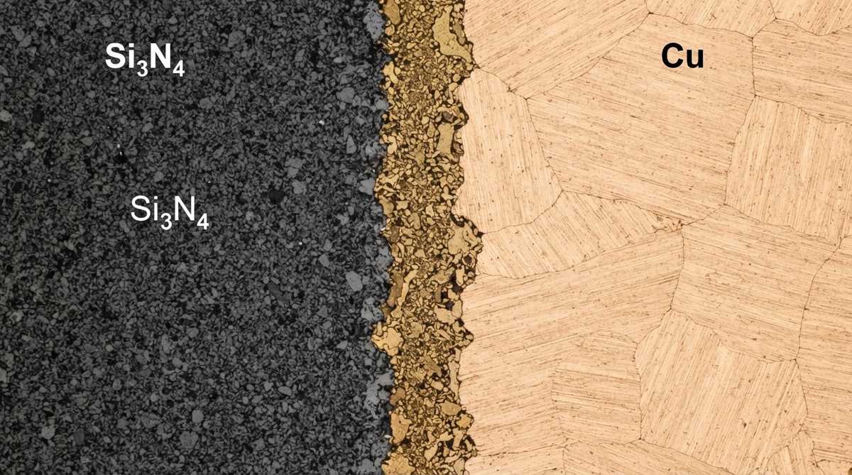
Silicon nitride Si3N4 PCB substrates are almost exclusively metallized using active metal brazing (AMB). In AMB, a titanium-containing braze alloy (typically AgCuTi) reacts with the Si3N4 surface at 800–900 °C in a vacuum furnace, forming a TiN reaction layer that bonds copper foil directly to the ceramic. This creates a stronger bond than DBC (direct bonded copper), which relies on a Cu-O eutectic that does not wet Si3N4 as reliably.
AMB on Si3N4 supports copper thicknesses from 0.15 mm to 0.8 mm per side. The bond strength exceeds 8 N/mm (peel test per DIN EN 2243-2), and the interface remains intact through thousands of thermal cycles. For details on the full ceramic PCB manufacturing process, including AMB brazing steps, see the process overview.
HTCC and LTCC are not compatible with Si3N4. These co-firing processes require a green-tape ceramic that sinters at defined temperatures with embedded metallization. Si3N4 sintering requires gas-pressure conditions (GPS or HIP) and temperatures above 1,700 °C that are incompatible with co-fired metal pastes.
Sourcing Si3N4 PCBs: What to Specify
When requesting quotes for a silicon nitride Si3N4 PCB, include these parameters in your specification:
- Substrate grade and source. Name the Si3N4 grade or specify minimum properties (e.g., KIC ≥ 6 MPa·√m, thermal conductivity ≥ 80 W/mK). Common grades include Kyocera SN series, CoorsTek FlexSiN, and Toshiba TSN-90.
- Substrate thickness. Standard options are 0.25 mm, 0.32 mm, and 0.64 mm. Thinner substrates reduce thermal resistance but are more fragile during handling.
- Copper thickness per side. Specify in mm: 0.15, 0.2, 0.3, 0.5, or 0.8 mm are typical. State whether symmetric or asymmetric.
- Circuit pattern. Provide Gerber files. Minimum trace/space depends on the AMB vendor; 0.3–0.5 mm is common.
- Surface finish. Ni/Au (electroless or electrolytic), Ni/Ag, or bare copper with OSP. Specify for solderability or wire-bonding requirements.
- Thermal-cycle qualification. State the cycle profile and minimum cycle count (e.g., −40 °C to +175 °C, 3,000 cycles per AQG 324).
For volume pricing and lead times on Si3N4 boards, the Si3N4 wholesale sourcing page covers MOQs and typical delivery schedules. If you need a lapped or polished surface for die-attach or thin-film metallization, see the polished and lapped Si3N4 substrate options.
When NOT to Use a Silicon Nitride Si3N4 PCB
Si3N4 is the wrong choice in several common scenarios:
- Cost-sensitive, moderate-reliability applications. If your thermal-cycle requirement is under 500 cycles at ΔT < 150 °C, 96% alumina substrates with DBC copper will meet the requirement at a fraction of the cost.
- Maximum thermal conductivity is the priority. If your design is heat-flux limited rather than reliability limited, aluminum nitride (AlN) PCBs at 170–200 W/mK will outperform Si3N4’s 70–90 W/mK.
- RF and microwave circuits. Si3N4’s dielectric constant (~8 at 1 MHz) and loss tangent (~0.002 at 1 GHz) are acceptable but not optimal. Alumina or specialized low-loss ceramics are better for RF signal integrity.
- Multilayer circuits. Si3N4 cannot be co-fired into multilayer ceramic PCBs. If you need embedded vias and internal routing, LTCC (alumina-based) or HTCC (alumina-based) are the appropriate technologies.
- Prototyping on a budget. For early-stage proof-of-concept work, start with AlN or alumina to validate the circuit, then move to Si3N4 for qualification and production if thermal-cycle testing demands it.
Frequently Asked Questions
Can I use DBC instead of AMB on Si3N4?
DBC bonding on Si3N4 is technically possible but uncommon. The Cu-O eutectic used in DBC does not wet Si3N4 as effectively as it wets alumina or AlN, resulting in lower bond strength and reduced thermal-cycle reliability. AMB with AgCuTi braze produces a TiN reaction layer that bonds more reliably. Most Si3N4 power module manufacturers have standardized on AMB.
What is the maximum continuous operating temperature for a Si3N4 PCB?
The Si3N4 ceramic itself retains structural integrity above 1,000 °C. The practical limit is set by the copper-braze interface, which is rated for continuous operation up to 300–350 °C depending on the braze alloy. Most designs operate with junction temperatures up to 200–250 °C.
How much does a Si3N4 substrate cost compared to AlN?
Si3N4 substrates typically cost 2–4× more than equivalent AlN substrates at comparable sizes and copper thicknesses. At volume (>1,000 pieces), the gap narrows somewhat. The cost premium is driven by the gas-pressure sintering process required for high-thermal-conductivity Si3N4 grades.
Is Si3N4 suitable for wire bonding?
Yes. Si3N4 AMB substrates with Ni/Au surface finish support both aluminum wedge bonding and gold ball bonding. The substrate’s mechanical rigidity provides a stable platform for ultrasonic bonding. Surface roughness should be specified below Ra 0.4 µm for reliable wire bonds.
What Si3N4 grades offer the highest thermal conductivity?
Toshiba TSN-90 and Kyocera SN-90 grades achieve 85–90 W/mK at 25 °C. These high-conductivity grades use controlled β-Si3N4 grain growth with rare-earth sintering aids (Y2O3, MgO) to minimize phonon scattering at grain boundaries. Standard grades range from 70–80 W/mK.
Can Si3N4 substrates be laser-scribed for snap-apart panels?
Yes. Laser scribing with a CO2 or fiber laser creates V-grooves on the substrate surface, allowing individual circuits to be separated after component assembly. Scribe depth is typically 30–50% of substrate thickness. This is standard practice for panel-format Si3N4 power module substrates.