Silicon nitride Si3N4 thin substrate material delivers 70–90 W/mK thermal conductivity and flexural strength above 700 MPa—a combination no other commercial ceramic matches. That mechanical toughness is the reason silicon nitride Si3N4 thin substrate technology dominates in power electronics where substrates must survive tens of thousands of thermal cycles without cracking.
Key Takeaways
- Si3N4 thin substrates are commercially available from 0.2 mm to 1.0 mm thickness, with 0.32 mm being the most common power-module grade.
- Fracture toughness of 6–7 MPa·√m is roughly 3× that of alumina (96% Al2O3) and 4× that of AlN, per CoorsTek and Kyocera datasheets.
- Thermal conductivity ranges from 70 W/mK (standard grade) to 90 W/mK (high-purity grade) at 25 °C, measured per ASTM E1461 (laser flash).
- Si3N4 is metallized via AMB (active metal brazing) or DBC (direct bonded copper); HTCC and LTCC processes are not used with this material.
- Cost per unit area is 3–8× higher than 96% alumina, making Si3N4 a poor fit for low-power or cost-sensitive designs.
What Is a Silicon Nitride Si3N4 Thin Substrate?
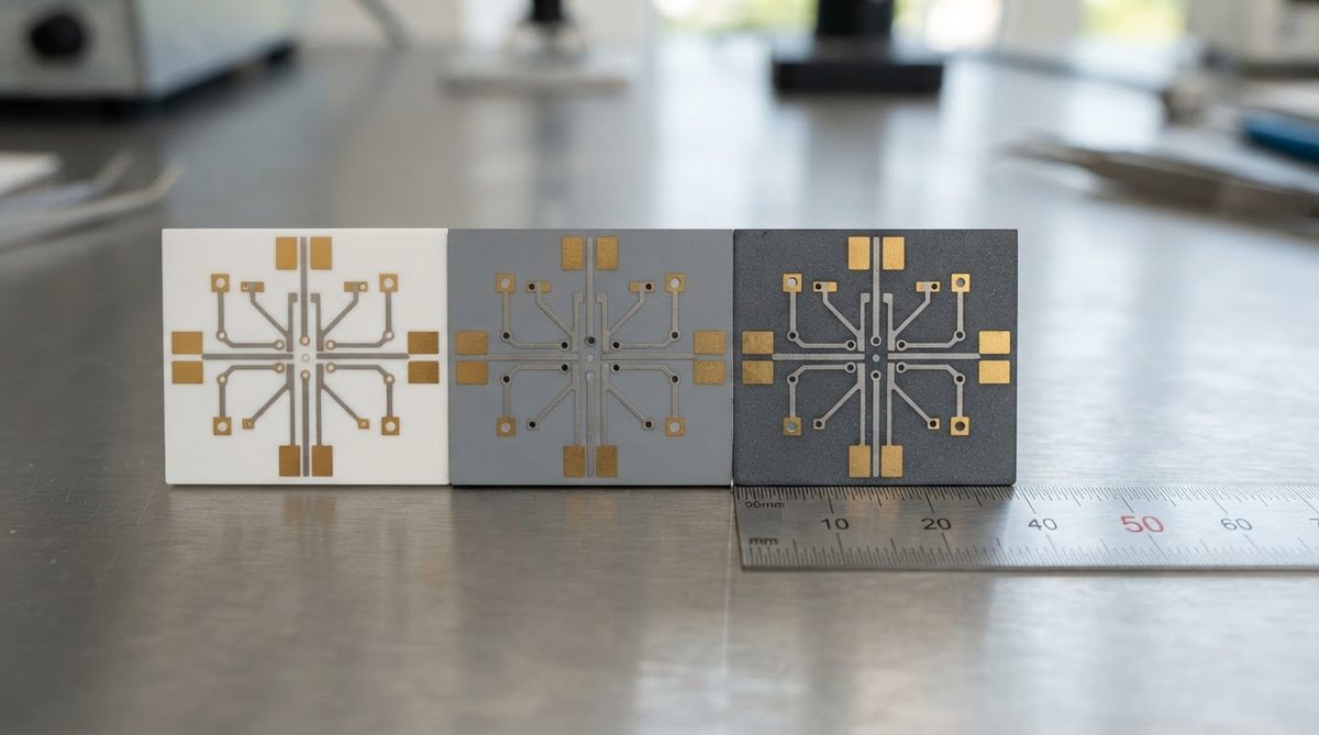
A silicon nitride Si3N4 thin substrate is a flat, dense ceramic sheet made from β-Si3N4 grains sintered with oxide additives (typically Y2O3 and MgO). “Thin” in this context means thicknesses at or below 1.0 mm. The material’s elongated grain microstructure creates an interlocking network that resists crack propagation far better than the equiaxed grains found in alumina or aluminum nitride.
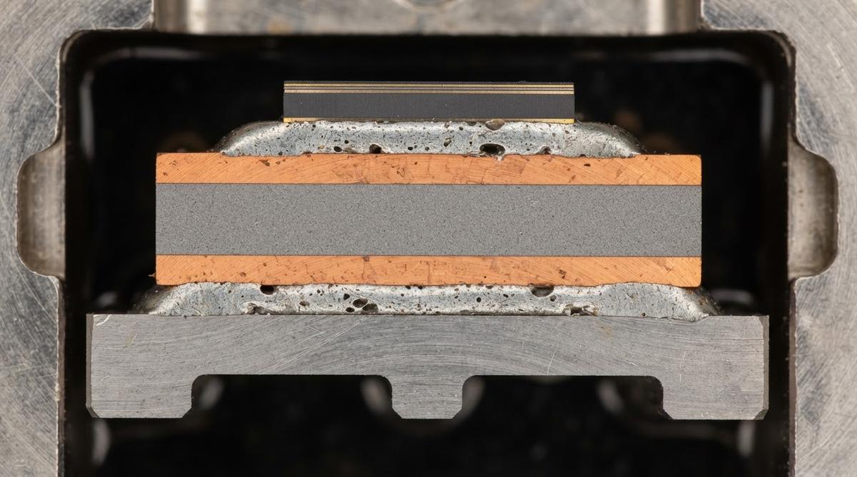
These substrates serve as the electrical insulator and heat spreader between a power semiconductor die and a copper baseplate. They are not used as standalone PCBs in the FR-4 sense; they become functional circuit carriers only after copper is bonded to one or both faces via Si3N4 AMB (active metal brazing) or Si3N4 DBC (direct bonded copper) processes.
Silicon Nitride Si3N4 Thin Substrate Property Table
| Parameter | Standard Grade | High-Purity Grade | Unit | Condition / Standard | Source |
|---|---|---|---|---|---|
| Thermal conductivity | 70 | 85–90 | W/mK | 25 °C, ASTM E1461 | Kyocera SN-733 / Toshiba TSN-90 |
| Flexural strength | 700–800 | 800–900 | MPa | 3-point bend, ASTM C1161 | Kyocera SN-733 datasheet |
| Fracture toughness (KIC) | 6.0–6.5 | 6.5–7.0 | MPa·√m | SEVNB, 25 °C | CoorsTek / Kyocera |
| Dielectric strength | 15–17 | 15–17 | kV/mm | AC, 60 Hz, IEC 60243 | Kyocera SN-733 |
| CTE | 2.7–3.0 | 2.7–3.0 | ppm/°C | 25–400 °C | Kyocera / Maruwa |
| Density | 3.20–3.25 | 3.20–3.25 | g/cm³ | Archimedes, ASTM C373 | Kyocera |
| Available thickness | 0.2, 0.32, 0.5, 0.635, 1.0 | 0.2, 0.32, 0.5, 0.635, 1.0 | mm | — | Multiple suppliers |
Typical values for commercially available material, for comparison only. Confirm against the datasheet for your specific grade.
How Si3N4 Compares to AlN and Alumina Thin Substrates
Choosing between a silicon nitride Si3N4 thin substrate, an AlN substrate, and an alumina substrate comes down to a three-way trade-off: thermal conductivity, mechanical reliability, and cost. The table below puts the numbers side by side for the most common thin-substrate grades.
| Parameter | Si3N4 (90 W/mK grade) | AlN (170–200 W/mK) | Al2O3 96% | Unit |
|---|---|---|---|---|
| Thermal conductivity (25 °C) | 85–90 | 170–200 | 24–28 | W/mK |
| Flexural strength | 800–900 | 300–400 | 350–380 | MPa |
| Fracture toughness | 6.5–7.0 | 2.5–3.0 | 3.5–4.0 | MPa·√m |
| CTE | 2.7–3.0 | 4.5–5.0 | 7.0–8.0 | ppm/°C |
| Relative cost (per cm²) | 5–8× | 3–5× | 1× (baseline) | — |
| Thermal-cycle life (ΔT = 200 °C, DBC) | >30,000 | ~3,000–5,000 | ~2,000–4,000 | cycles to first crack |
Cycle-life figures are order-of-magnitude ranges from published Infineon and Fuji Electric reliability reports. Actual results depend on copper thickness, solder, and die-attach method.
AlN wins on raw thermal conductivity. But in applications with wide temperature swings—EV traction inverters, railway converters, wind-turbine power stacks—the substrate that cracks first is the substrate that fails first. The silicon nitride Si3N4 thin substrate’s fracture toughness makes it the default choice whenever thermal-cycle reliability is the primary design driver. For a deeper look at how thermal conductivity varies with grade and sintering, see the guide on Si3N4 thermal conductivity.
Worked Example: Thermal Resistance Through a 0.32 mm Si3N4 Substrate
Consider a 10 mm × 10 mm die on a 0.32 mm silicon nitride Si3N4 thin substrate (90 W/mK grade). One-dimensional thermal resistance through the ceramic alone:
Rth = t / (k × A) = 0.00032 m / (90 W/mK × 0.0001 m²) = 0.036 °C/W
For comparison, the same geometry in AlN (180 W/mK) gives 0.018 °C/W, and in 96% alumina (26 W/mK) gives 0.123 °C/W. The Si3N4 substrate adds roughly twice the thermal resistance of AlN but still keeps the ceramic contribution well below the die-attach and heat-sink interface resistances, which typically total 0.2–0.5 °C/W in a power module. For many designs, the 0.018 °C/W difference between Si3N4 and AlN is negligible compared to the reliability gain.
Enter your own substrate dimensions, material grade, and dissipated power below to estimate junction temperature rise for any ceramic type.
Typical Applications for Si3N4 Thin Substrates
- EV traction inverters — SiC MOSFET modules running at junction temperatures up to 175 °C with coolant ΔT swings of 100–150 °C.
- Railway power converters — IGBT modules with 30-year service life requirements and millions of thermal cycles.
- Wind-turbine converters — Remote installations where module replacement cost dwarfs substrate cost.
- Aerospace and defense power supplies — Vibration and thermal shock environments that crack brittle ceramics.
To compare Si3N4 against other ceramic substrate materials, including alumina and AlN grades, the material comparison page provides side-by-side property data.
When NOT to Use Si3N4 Thin Substrates
A silicon nitride Si3N4 thin substrate is overkill—and overpriced—in several common scenarios:
- Steady-state thermal loads with mild cycling (ΔT < 60 °C): AlN or even 96% alumina on DBC will survive the required cycle count at a fraction of the cost.
- High-frequency RF circuits: Si3N4’s dielectric constant (~8) and loss tangent are higher than alumina 99.6% or AlN. AlN thin-film substrates or 99.6% alumina are better RF choices.
- Low-power LED or sensor boards: An alumina thin-film substrate at 0.25 mm handles the heat and costs 5–8× less.
- Budget-constrained prototyping: Use AlN DBC for early validation, then switch to Si3N4 for qualification and production if cycle-life data demands it.
Frequently Asked Questions
How thin can you get a Si3N4 substrate?
Commercial Si3N4 substrates are available as thin as 0.2 mm (200 µm). At this thickness, the material retains flexural strength above 700 MPa, which is still roughly double that of a 0.635 mm AlN substrate. Handling 0.2 mm sheets requires vacuum tooling to avoid edge chipping.
Can Si3N4 be processed with HTCC or LTCC?
No. Si3N4 requires gas-pressure sintering at 1,700–1,900 °C under nitrogen atmosphere, which is incompatible with HTCC and LTCC co-firing processes. Metallization is done after sintering, via AMB or DBC.
Does Si3N4 cost more than AlN?
Yes. Si3N4 substrates typically cost 1.5–2× more than equivalent AlN substrates and 5–8× more than 96% alumina, depending on grade and volume. The cost premium is justified when thermal-cycle reliability requirements exceed what AlN can deliver. For volume pricing, see Si3N4 substrate wholesale pricing.
What copper thickness can be bonded to Si3N4?
AMB can bond copper foils from 0.15 mm to 0.8 mm onto Si3N4. DBC on Si3N4 typically uses 0.2–0.4 mm copper. Thicker copper increases current capacity but also raises thermal-cycle stress at the copper-ceramic interface; AMB handles this better than DBC for copper above 0.4 mm.
Is Si3N4 suitable for double-sided metallization?
Yes. Both AMB and DBC processes can metallize both faces of a Si3N4 thin substrate in a single furnace run. Double-sided metallization is standard in power-module designs where one side carries the circuit pattern and the other is a continuous ground plane brazed to a baseplate.