Knowing how to cut ceramic substrate correctly depends on three things: the material (Al₂O₃, AlN, or Si₃N₄), the tolerance you need, and whether you are prototyping or running production. Laser cutting delivers the tightest kerf and best edge quality for most ceramics; diamond scribing is cheapest for straight-line singulation of large panels; and diamond sawing handles thick substrates that lasers cannot penetrate in a single pass. Below is a practical comparison of all five common methods so you can match the cut to your board.
Key Takeaways
- Nd:YAG and UV laser cutting produces a kerf of 20–50 µm with a heat-affected zone (HAZ) under 30 µm on 96 % alumina up to ~1.0 mm thick.
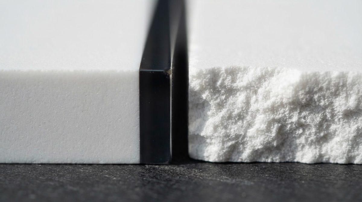
- Diamond scribe-and-snap is the lowest-cost way to cut ceramic substrate along straight lines, but it cannot cut curves and leaves a rougher edge (Ra 3–6 µm vs. <1.5 µm for laser).
- Abrasive waterjet cuts any ceramic thickness without thermal stress, but kerf width (200–400 µm) wastes more material and positional accuracy is ±0.1 mm at best.
- Si₃N₄ resists fracture during mechanical scribing far better than alumina due to its higher fracture toughness (5–7 MPa·√m vs. 3–4 MPa·√m for 96 % Al₂O₃), but it absorbs UV laser wavelengths less efficiently, requiring slower feed rates.
- Post-cut cleaning matters: laser cutting leaves a recast layer 5–15 µm deep that can degrade solder wetting if not removed by ultrasonic cleaning or light lapping.
Why Ceramic Substrate Is Harder to Cut Than FR-4
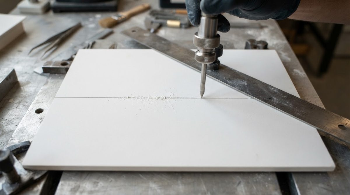
FR-4 is a glass-epoxy composite with a Vickers hardness around 3–4 GPa. Alumina sits at 14–16 GPa (96 %) and aluminum nitride at 11–13 GPa, per CoorsTek published datasheets. That hardness, combined with brittleness (low fracture toughness), means conventional routing bits dull in seconds and shear forces can propagate cracks well beyond the cut line. Every method used to cut ceramic substrate either avoids mechanical contact altogether (laser, waterjet) or uses a tool harder than the substrate (diamond).
If you are still selecting a ceramic substrate type, factor in machinability early. AlN machines more cleanly under laser than Al₂O₃ at the same thickness, and silicon nitride tolerates mechanical scribing with fewer micro-cracks thanks to its interlocking grain structure.
Five Methods: How to Cut Ceramic Substrate for Different Needs
1. Nd:YAG / UV Laser Cutting
A focused beam (typically 355 nm UV or 1064 nm Nd:YAG, pulsed at 10–100 kHz) ablates ceramic in successive passes. UV wavelengths couple better with Al₂O₃, giving a cleaner cut with less micro-cracking. Kerf width is 20–50 µm. Positional accuracy reaches ±10–25 µm on modern galvo-scanner systems.
Laser is the go-to for complex outlines, tight tolerances, and thin substrates (0.25–0.635 mm). It struggles above ~1.0 mm on alumina because multiple passes accumulate heat, widening the HAZ. For thicker substrates, a two-step approach—laser scribe to half-depth, then mechanical snap—often works better. AluminaPCB offers laser-cut ceramic substrates for custom shapes and small-to-mid volumes.
2. Diamond Scribe-and-Snap
A diamond-tipped stylus scores a groove 30–50 % of the substrate thickness along a straight line. The panel is then flexed over a breaking bar. This is the standard method for ceramic PCB singulation of rectangular units from a larger panel.
Advantages: fast cycle time (~0.5 s per scribe line), no consumable gas or water, minimal capital cost. Disadvantages: straight lines only, edge roughness Ra 3–6 µm, risk of chipping on substrates thinner than 0.25 mm or thicker than 1.0 mm. Scribe depth must be tightly controlled; too shallow and the snap wanders, too deep and the substrate cracks prematurely during handling.
3. Diamond Blade Dicing Saw
A resin- or metal-bonded diamond blade spinning at 20 000–40 000 rpm cuts through the full substrate thickness with coolant flood. Kerf width is 100–300 µm depending on blade thickness. Positional accuracy is ±25–50 µm. This method handles substrates up to 2 mm thick without difficulty.
Dicing saws are common in semiconductor packaging lines, so many facilities already own one. The trade-off is blade wear: cutting 96 % alumina wears a blade roughly 3–5× faster than cutting silicon, per typical consumable life data from Disco Corporation. Blade cost per cut matters at volume.
4. Abrasive Waterjet
A 60 000–90 000 psi water stream loaded with garnet abrasive (80–120 mesh) erodes through any ceramic at any thickness. No thermal stress, no HAZ. Kerf width is 200–400 µm—the widest of all five methods. Positional accuracy is ±0.1–0.15 mm, adequate for mechanical outlines but not fine features.
Waterjet is best for thick (>1 mm) substrates, prototypes, and shapes where thermal damage is unacceptable. It is the slowest method on thin substrates and wastes the most material per cut.
5. CO₂ Laser Scribe-and-Snap
A CO₂ laser (10.6 µm wavelength) heats a narrow line on the ceramic surface, then a coolant jet (air or water mist) quenches it. The thermal shock creates a controlled crack along the scribed path. The panel is then snapped. This method is fast and produces a clean edge on alumina up to ~1.0 mm, but it only works for straight or gently curved lines and is poorly suited to AlN, which has high thermal conductivity that dissipates the thermal gradient before a crack initiates.
Comparison Table: How to Cut Ceramic Substrate by Method
| Parameter | Nd:YAG / UV Laser | Diamond Scribe | Diamond Saw | Waterjet | CO₂ Scribe-Snap |
|---|---|---|---|---|---|
| Kerf width | 20–50 µm | ~0 (snap line) | 100–300 µm | 200–400 µm | ~0 (snap line) |
| Positional accuracy | ±10–25 µm | ±50–100 µm | ±25–50 µm | ±100–150 µm | ±50–100 µm |
| Edge roughness (Ra) | 0.8–1.5 µm | 3–6 µm | 1.5–3 µm | 3–8 µm | 1–3 µm |
| Max practical thickness | ~1.0 mm (single pass) | 0.25–1.0 mm | >2 mm | Any | ~1.0 mm |
| Curved / complex outlines | Yes | No | Limited | Yes | No |
| Heat-affected zone | 10–30 µm | None | Minimal | None | 10–50 µm |
| Best-fit material | Al₂O₃, AlN | Al₂O₃ | All | All | Al₂O₃ |
| Relative cost per cut (low vol.) | Medium | Low | Medium | High | Low–Medium |
Typical values for commercially available equipment and substrates, for comparison only. Confirm against your equipment specs and substrate datasheet for your specific grade.
Worked Example: Tolerance Stack for a Laser-Cut 10 × 10 mm Substrate
Suppose you need a 10.00 × 10.00 mm Al₂O₃ 96 % substrate, 0.635 mm thick, cut from a standard 4.5″ × 4.5″ panel. Your assembly requires ±0.05 mm on the finished part.
- Laser positional accuracy: ±0.025 mm (from machine spec).
- Kerf half-width variation: ±0.010 mm (beam stability over the run).
- Substrate flatness / clamping error: ±0.010 mm.
- RSS total: √(0.025² + 0.010² + 0.010²) = √(0.000625 + 0.0001 + 0.0001) ≈ ±0.029 mm.
The RSS result of ±0.029 mm sits well inside your ±0.05 mm budget. If you switched to diamond scribe-and-snap (±0.075 mm positional), the stack would blow past the tolerance. This is a common reason engineers choose laser when they need to cut ceramic substrate to tight dimensions.
Enter your substrate dimensions, thickness, and required tolerance below to see which cutting method meets your accuracy budget.
How to Choose the Right Method to Cut Ceramic Substrate
Run through this decision sequence:
- Is the outline curved or has internal cutouts? → Laser or waterjet. Everything else is straight-line only (or nearly so).
- Is the substrate thicker than 1.0 mm? → Diamond saw or waterjet. Laser requires multiple slow passes; scribe-and-snap becomes unreliable.
- Do you need positional accuracy tighter than ±0.05 mm? → Laser. Nothing else hits that window consistently.
- Is it a high-volume rectangular singulation from panels? → Diamond scribe-and-snap for lowest cost per unit.
- Is the material AlN? → Prefer Nd:YAG/UV laser or diamond saw. CO₂ scribe-snap is ineffective on AlN due to its high thermal conductivity (170–200 W/mK).
Post-Cut Processing You Should Not Skip
Cutting is not the last step. Laser-cut edges carry a recast layer (re-solidified ceramic) that is amorphous and porous. If you plan to metallize or solder near the edge, remove this layer by ultrasonic cleaning in DI water followed by a brief lapping or tumbling pass. Diamond-sawed edges pick up blade-bonding residue; an ultrasonic clean in isopropanol handles this.
Inspect cut edges under 20× magnification for micro-cracks that extend more than 50 µm from the cut line. On Al₂O₃ 96 %, cracks longer than 100 µm can propagate under thermal cycling (per ASTM C1161 flexural strength testing guidance). Reject or re-cut any substrate with visible edge chipping wider than 0.1 mm.
When Not to Cut Ceramic at All
If your design allows it, order substrates pre-cut to final dimensions from the manufacturer. Pre-fired (green-state) cutting is far easier and cheaper than cutting sintered ceramic. Tolerances on green-cut parts after sintering are ±0.5–1.0 % of the dimension due to shrinkage variation, so this only works when your tolerance budget is loose (>±0.1 mm on a 10 mm part). For tighter tolerances, post-sinter cutting is unavoidable.
If your part is rectangular and a standard thickness, buying pre-singulated blanks eliminates cutting entirely and removes a failure mode from your process.
Frequently Asked Questions
Can I cut ceramic substrate with a Dremel or rotary tool?
Yes, but only for rough prototyping. A diamond-coated cutoff wheel on a rotary tool will cut thin alumina (≤0.635 mm), but edge quality is poor (Ra >10 µm), chipping is common, and dimensional accuracy depends entirely on hand steadiness. Do not use this method for parts that will be metallized or assembled.
Does cutting ceramic substrate create hazardous dust?
Alumina and AlN dust are classified as nuisance particulates, not toxic, but prolonged inhalation of fine ceramic dust can cause respiratory irritation. Use wet cutting or vacuum extraction. If you are cutting beryllium oxide, stop—BeO dust is a confirmed human carcinogen and requires full OSHA-compliant engineering controls. See the beryllia safety guide before handling BeO in any form.
How do I hold a thin ceramic substrate during cutting?
Vacuum chucks work best for substrates 0.25–0.50 mm thick. Mechanical clamps risk cracking brittle ceramics. For laser cutting, a sacrificial backing plate (aluminum or stainless steel) beneath the substrate prevents exit-side chipping and absorbs the residual beam energy.
What is the cheapest way to cut ceramic substrate for a prototype?
Diamond scribe-and-snap using a handheld carbide or diamond scriber costs under $20 in tooling and works on Al₂O₃ up to about 0.635 mm thick for straight cuts. Score to roughly 40 % depth, place the score line over a straight edge, and press down firmly on both sides. Expect ±0.2 mm accuracy and some edge chipping.
Can I laser-cut a ceramic substrate that already has copper metallization?
Yes, but copper reflects the 1064 nm Nd:YAG wavelength efficiently, so the laser must first ablate through the copper (which requires higher peak power or a UV wavelength) before cutting the ceramic beneath. This increases HAZ near the copper-ceramic interface. Many manufacturers prefer to cut ceramic substrate first and metallize afterward. If your process requires post-metallization cutting, discuss the copper thickness and layout with your laser operator to set appropriate parameters.
Does substrate purity affect how cleanly it cuts?
Higher-purity alumina (99.6 % vs. 96 %) has a more uniform grain structure and fewer glassy-phase inclusions, which reduces micro-chipping during mechanical cutting and produces a more consistent laser ablation rate. The difference is measurable but modest—expect roughly 10–20 % less edge chipping on 99.6 % alumina under identical saw conditions. More detail is available in the purity and performance guide.