Laser Drilling Definition
A clear laser drilling definition starts here: laser drilling is a non-contact machining process that uses a focused laser beam to ablate material and form holes in a ceramic substrate. In ceramic PCB fabrication, it is the primary method for creating vias and through-holes in hard, brittle materials such as Al₂O₃, AlN, and Si₃N₄ that would crack or chip under mechanical drill bits.
How Laser Drilling Works
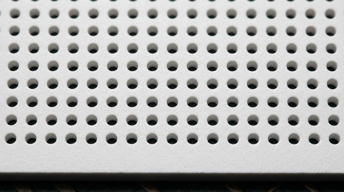
A pulsed laser—most often a CO₂ (10.6 µm wavelength) or UV Nd:YAG (355 nm)—delivers short bursts of energy to the substrate surface. Each pulse vaporises a small volume of ceramic. The beam is positioned by galvanometer mirrors or an XY stage, and the pulse count and energy are tuned to control hole depth and diameter.
CO₂ lasers are efficient for larger holes (≥ 100 µm) in alumina. UV lasers produce smaller spot sizes and less peripheral heat, making them the better choice for microvias below 80 µm or for AlN substrates where thermal shock cracking is a concern. Understanding this distinction is essential to applying the laser drilling definition in practice.
The basic sequence for laser drilling a ceramic substrate follows these steps:
- The substrate is fixtured on a vacuum chuck to prevent movement.
- A vision system aligns fiducial marks to the drill program.
- The laser fires a controlled number of pulses at each hole location, ablating ceramic layer by layer.
- Debris is removed by an assist gas (typically compressed air or nitrogen).
- Drilled holes are inspected optically for diameter, taper, and edge quality.
Typical Capabilities
| Parameter | CO₂ Laser | UV Nd:YAG Laser |
|---|---|---|
| Minimum hole diameter | ~80–100 µm | ~25–50 µm |
| Position accuracy | ±15–25 µm | ±5–10 µm |
| Typical substrate materials | Al₂O₃ 96 %, Al₂O₃ 99.6 % | Al₂O₃, AlN, Si₃N₄ |
| Heat-affected zone | Moderate | Minimal |
Values are representative of industry equipment. Confirm against your fabricator’s process sheet.
Why Laser Drilling Matters for Ceramic PCBs
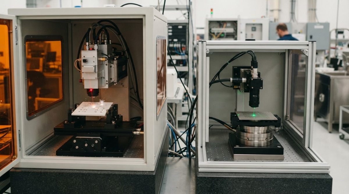
Ceramic substrates are too hard (Vickers hardness > 1,000 HV for alumina) for conventional carbide drill bits at production volumes. Laser drilling eliminates tool wear entirely and avoids the micro-cracking that mechanical contact can cause. After laser drilling, holes are typically filled with conductive paste via screen printing and then co-fired or post-fired to form electrical vias.
Limitations of Laser Drilling
No single process fits every situation. Laser drilling is slower per hole than mechanical drilling in soft materials like FR-4. Hole taper increases with substrate thickness; aspect ratios above 5:1 are difficult without specialised optics. Very thick substrates (> 1 mm) may need multiple passes, which increases cycle time and cost. For large-diameter holes (> 0.5 mm), mechanical punching of green-state LTCC tape before sintering is often faster and cheaper than laser drilling of fired ceramic.
FAQ
Can laser drilling cut slots or cavities, not just round holes?
Yes. By tracing a path with overlapping pulses, a laser can cut slots, rectangles, and complex cavity shapes in ceramic substrates. Cycle time scales with the perimeter length.
Does laser drilling damage the surrounding ceramic?
UV lasers produce a heat-affected zone of only a few micrometres, so damage is minimal. CO₂ lasers generate more peripheral heat and may cause micro-recast layers that need cleaning before metallisation.
Is laser drilling used on green or fired ceramic?
Both. LTCC green tape is often mechanically punched, but fired alumina and AlN substrates are almost always laser-drilled because they are too hard for mechanical tooling.