Thin Film Definition: What It Means in Ceramic PCB Engineering
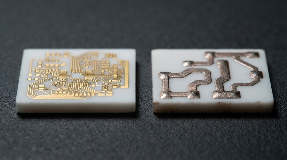
The thin film definition used across the ceramic PCB industry refers to a vacuum-based metallization technique that deposits one or more metal layers—typically less than 2 µm thick—onto a ceramic substrate using sputtering or electron-beam evaporation. The deposited metal is then photo-lithographically patterned and etched to create conductor traces, resistors, or capacitor electrodes with line widths as fine as 10–25 µm.
Because the metal is applied atom-by-atom in a controlled vacuum, thin film produces smoother, denser, and more dimensionally precise conductors than screen-printed ceramic PCB manufacturing methods like thick film. This precision matters most in high-frequency RF circuits, thin-film resistor networks, and sensors where tight impedance control or sub-mil feature sizes are required.
How the Thin Film Definition Separates It from Thick Film
| Parameter | Thin Film | Thick Film |
|---|---|---|
| Deposition method | Sputtering / evaporation (vacuum) | Screen printing (paste) |
| Typical metal thickness | 0.1–2 µm (before plating) | 10–25 µm (fired) |
| Minimum trace / space | 10–25 µm | 100–150 µm |
| Surface roughness (Ra) | < 0.05 µm | 0.5–1.5 µm |
| Resistor tolerance | ±0.1–1 % | ±5–10 % (as-fired) |
| Cost per board | Higher (vacuum tooling) | Lower (screen + kiln) |
The table above captures the core of the thin film definition in practice: vacuum deposition, sub-micron roughness, and lithographic patterning that together enable feature sizes an order of magnitude finer than thick film. Thin film traces are often plated up with additional copper or gold after the initial vacuum deposition to reach the current-carrying thickness a design needs. Review thin film copper thickness and capabilities for specifics on achievable build-ups.
Common Substrate Materials for Thin Film
Thin film metallization is most commonly applied to alumina and aluminum nitride ceramics. 96% alumina thin film substrates serve as the cost-effective baseline, while 99.6% alumina and AlN are chosen when tighter surface finish or higher thermal conductivity is needed. The substrate surface must be polished to Ra < 0.05 µm before deposition; rough surfaces degrade adhesion and line definition.
Understanding the thin film definition also means understanding substrate preparation. Unlike thick film, where paste fills minor surface irregularities during firing, thin film faithfully replicates every surface defect. A scratch or pit on the ceramic becomes a break or pinch-point in the conductor.
Typical Applications
- RF and microwave circuits (filters, couplers, matching networks) up to 77 GHz and beyond
- Precision thin-film resistor networks for instrumentation
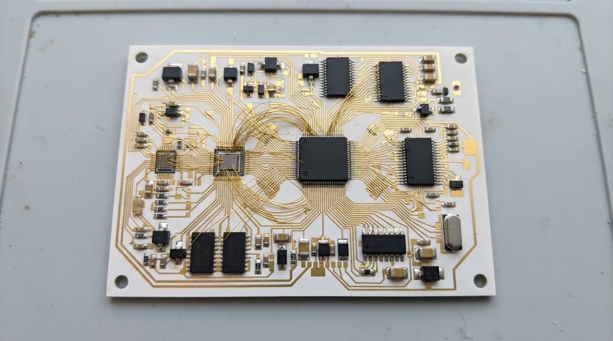
- Hybrid modules combining thin film traces with wire-bonded bare die
- MEMS sensor packaging and interposers
When Thin Film Is Not the Right Choice
If your design needs only 150 µm traces and ±5 % resistors, thick film will cost less and ship faster. For high-current power circuits requiring 100+ µm copper, DBC or DPC processes are more practical. The thin film definition centers on precision—if your tolerances don’t demand it, the vacuum processing cost is hard to justify.
Frequently Asked Questions
What does the thin film definition mean in simple terms?
A thin film is a metal layer under 2 µm thick deposited onto a substrate in a vacuum using sputtering or evaporation, then patterned with photolithography. The process produces conductors and resistors with much finer features and tighter tolerances than screen-printed thick film methods.
How thin is a thin film layer compared to thick film?
Thin film layers are typically 0.1–2 µm before any plating step, roughly 10–100× thinner than thick film conductors at 10–25 µm fired thickness. After plating, thin film traces can reach several microns but still start from a vacuum-deposited seed layer.
Can thin film resistors replace discrete SMD resistors?
Yes, in many precision applications. Thin film resistors deposited directly on the ceramic substrate achieve tolerances of ±0.1–1 % and temperature coefficients under ±25 ppm/°C, which matches or exceeds many discrete chip resistors while eliminating solder joints and saving board area.
Is thin film more expensive than thick film?
Thin film costs more per board because it requires vacuum deposition equipment, cleanroom-grade substrate polishing, and photolithographic patterning. The premium is justified when a design demands trace widths below 100 µm, resistor tolerances tighter than ±1 %, or surface roughness below 0.05 µm Ra.