Ceramic PCB ESD handling requires stricter protocols than standard FR-4 workflows because bare alumina holds charge indefinitely. A 96% Al₂O₃ substrate has surface resistivity above 10¹⁴ Ω, meaning charge deposited on an unmetallized area can sit for minutes without dissipating. A single discharge event can blow thin-film traces, punch through dielectric layers, or cause latent damage that only shows up weeks later in the field. Every facility assembling ceramic boards needs ionizers, grounded fixtures, and shielding packaging beyond what ANSI/ESD S20.20 requires for organic substrates.
Why Ceramic PCB ESD Handling Demands Extra Attention
On an FR-4 board, absorbed moisture lowers surface resistivity enough to bleed off minor charges passively. Ceramic does not absorb moisture. A 96% alumina substrate at 25 °C and 40% RH maintains surface resistivity above 10¹⁴ Ω (per CoorsTek datasheet for ADS-96R). That stored charge concentrates at metallization edges and via transitions, exactly where thin-film or DBC copper traces are thinnest and most vulnerable.
Thin-film metallizations (sputtered TiW/Au, NiCr/Au) used in RF and sensor applications are typically 0.1–5 µm thick. At that scale, an ESD pulse of even 100 V across a narrow gap can vaporize a trace segment. Thick-film conductors (10–25 µm screen-printed Ag or AgPd) tolerate higher energy but are still at risk from human-body-model (HBM) discharges averaging 2–4 kV.
ESD Workstation Requirements for Ceramic Boards
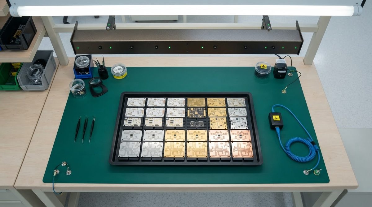
Follow ANSI/ESD S20.20 as the baseline standard. The table below lists the specific items and their required performance levels for proper ceramic PCB ESD handling.
| Item | Requirement | Standard |
|---|---|---|
| ESD mat (bench) | Surface resistance 10⁶–10⁹ Ω | ANSI/ESD S4.1 |
| Wrist strap | Total system resistance < 35 MΩ | ANSI/ESD S1.1 |
| Heel grounders / shoe straps | Total resistance < 100 MΩ | ANSI/ESD S9.1 |
| ESD flooring | Surface resistance 10⁶–10⁹ Ω | ANSI/ESD S7.1 |
| Ionizer (overhead) | Offset voltage < ±25 V, decay < 2 s to 50 V | ANSI/ESD SP3.3 |
| Humidity | 40–60% RH recommended | IEC 61340-5-1 |
| Packaging (transport) | Shielding bag, < 50 V charge on inner surface | ANSI/ESD S541 |
Values per ANSI/ESD S20.20-2021 and referenced component standards.
An overhead ionizer is optional for FR-4 workflows but strongly recommended for ceramic substrates. Because the bare ceramic surface cannot dissipate charge conductively, an ionizer is the only way to neutralize charge that accumulates on unmetallized regions during handling.
Step-by-Step Ceramic PCB ESD Handling Procedure
- Incoming inspection. Open shipping containers only at a grounded ESD workstation. Ceramic substrates from the factory ship in conductive or static-shielding trays. Do not transfer them to standard plastic bins.
- Visual and dimensional check. Wear a grounded wrist strap. Hold substrates by edges only; fingerprint oils on metallized pads degrade solder wetting later. Use powder-free nitrile gloves if the process requires bare-hand contact.
- Storage. Keep boards in their original ESD-safe packaging inside a dry cabinet (≤ 10% RH) or nitrogen-purged container. For detailed storage guidance, see ceramic PCB storage conditions and shelf life.
- Solder paste application / component placement. Ground all automated equipment (stencil printer, pick-and-place) per ANSI/ESD S20.20. Verify grounding daily with a surface resistance meter.
- Reflow / wire bonding. The reflow oven itself is grounded, but loading and unloading are high-risk moments. Use grounded carriers or fixtures. Never slide a ceramic board across any surface; the triboelectric charge generated by alumina against most polymers exceeds 5 kV easily.
- Final test and pack-out. Discharge test probes before contacting pads. Package finished assemblies in ESD shielding bags with desiccant if the product will be stored before shipment.
Use the derating tool below to check whether your operating temperature affects the surface resistivity assumptions in your ESD control plan. Enter your substrate material and ambient temperature to see how resistivity shifts.
Common Mistakes That Cause ESD Damage on Ceramic Boards
Sliding boards out of trays. Pulling a ceramic substrate across a plastic tray generates triboelectric charge. Alumina sits high on the triboelectric series (positive end), so contact with PTFE, polyethylene, or polypropylene produces large charge separation. Lift boards straight up instead.
Using compressed air to clean. Unionized compressed air creates charge through the triboelectric effect of gas flow across an insulating surface. Use ionized air guns rated per ANSI/ESD SP3.3, or clean with isopropanol wipes at a grounded station.
Skipping ionizers because “the board is grounded through the fixture.” Only the metallized areas are grounded through the fixture. The ceramic itself remains an insulator. Charge on bare ceramic can arc to nearby traces at any time. Proper ceramic PCB ESD handling always accounts for exposed insulating surfaces separately from grounded metal.
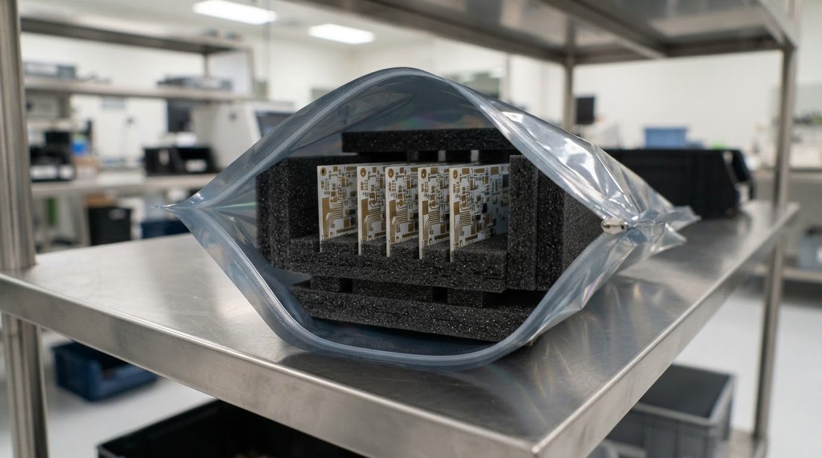
Storing bare substrates in standard cardboard boxes. Cardboard is triboelectrically active and not ESD-safe. Use conductive foam inserts inside ESD-shielding containers.
When ESD Precautions Alone Are Not Enough
If your design routes thin-film traces (< 1 µm) across large unmetallized ceramic areas, consider adding on-board ESD protection structures: spark gaps, TVS pads, or guard rings around sensitive nets. These are standard practice in RF hybrid circuits on alumina. The ceramic PCB FAQ covers related design questions.
For assemblies that will be handled repeatedly in the field (sensor modules, replaceable power stages), conformal coating over exposed metallization reduces the risk of field ESD events damaging traces after the board leaves your controlled environment.
When Standard FR-4 ESD Practices Are Sufficient
If your ceramic board is fully metallized on both sides with thick copper (DBC or AMB, > 100 µm Cu), the exposed ceramic area is minimal and the copper itself provides a conduction path for charge dissipation. In this case, standard FR-4-level ESD controls per IPC J-STD-033 are adequate. You do not need ionizers or special trays. The critical factor is the ratio of exposed insulating ceramic to grounded metal. Boards with large bare ceramic windows always need the enhanced ceramic PCB ESD handling protocol described above. For more on substrate types and metallization options, see the ceramic PCB overview.
Frequently Asked Questions
Can ESD crack a ceramic PCB?
ESD does not crack ceramic mechanically. The energy in a typical HBM discharge (roughly 0.4 µJ at 2 kV) is far too low to fracture alumina, which has a flexural strength of 300–380 MPa per ASTM C1161. ESD damages metallization and components, not the substrate itself.
Do I need a different ESD program for AlN versus alumina?
No. Aluminum nitride has similarly high surface resistivity (> 10¹⁴ Ω) and the same inability to bleed charge. Use the same ANSI/ESD S20.20-compliant workstation for both materials. The one difference: AlN substrates are more expensive, so the cost of a single ESD-damaged board is higher. For information on AlN material properties, see alumina and high-purity ceramic substrates.
What humidity level prevents ESD on ceramic?
Higher humidity helps dissipate charge from organic surfaces but has almost no effect on ceramic. Even at 70% RH, bare alumina surface resistivity stays above 10¹² Ω. Humidity control helps protect other materials in the assembly area but is not a substitute for ionizers and grounding when handling ceramic boards.
Should I ground myself when hand-soldering to a ceramic PCB?
Yes. Wear a grounded wrist strap and work on a grounded ESD mat. The soldering iron tip must also be grounded (verify < 2 Ω tip-to-ground). For solder alloy selection guidance, see which solder to use on ceramic substrates.
Can I reuse ESD shielding bags for ceramic boards?
Only if the bag passes a surface resistance check (10⁶–10¹¹ Ω per ANSI/ESD S541) and has no punctures. Ceramic edges are sharp enough to cut through thin shielding bags, so inspect bags carefully before reuse. When in doubt, use a new bag.