DBC direct bonded copper layout guidelines differ sharply from standard PCB design rules because the copper is 0.127–0.635 mm (5–25 mil) thick, the ceramic substrate is brittle, and thermal cycling stresses the copper-ceramic bond. DBC (direct bonded copper) substrates carry these heavy copper layers bonded directly to Al₂O₃ or AlN ceramic through a high-temperature copper-oxide eutectic process. The guidelines below give minimum dimensions, clearances, and design practices that keep DBC substrates manufacturable and reliable through thousands of thermal cycles.
Key Takeaways
- Minimum trace width for DBC is typically 0.3–0.5 mm, depending on copper thickness—roughly 3–10× wider than DPC or thin-film processes.
- Copper-to-edge clearance should be ≥0.5 mm to prevent delamination during scribing or dicing.
- Balanced copper coverage on top and bottom reduces bow and warp caused by CTE mismatch during thermal cycling.
- Corner radii on all copper features should be ≥0.3 mm; sharp 90° corners concentrate thermo-mechanical stress and initiate cracks.
- AlN substrates require tighter process control than Al₂O₃ because AlN’s higher thermal conductivity (170–200 W/mK) comes with greater sensitivity to oxidation during bonding.
How the DBC Process Shapes Layout Rules
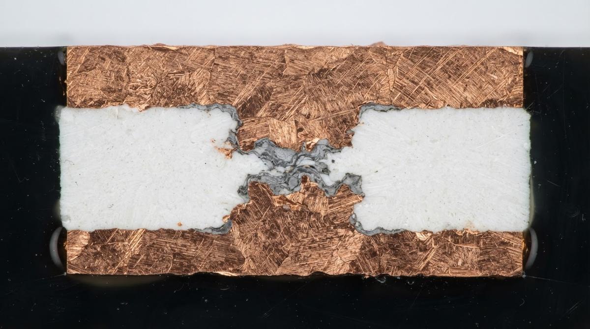
In DBC, a copper foil is placed on the ceramic and heated to roughly 1065–1083 °C in a controlled atmosphere. A thin copper-oxide layer at the interface forms a eutectic that wets the ceramic surface, creating a direct metallurgical bond. The copper is then etched to form the circuit pattern.
Because the bonded copper starts as a solid foil—not a plated or printed film—it is much thicker than traces produced by DPC (direct plated copper) processes or thin-film metallization. This thickness carries more current and spreads heat more effectively, but it also means the etch undercut is larger and the minimum feature size is coarser. Understanding this trade-off is central to applying DBC direct bonded copper layout guidelines correctly.
DBC Direct Bonded Copper Layout Guidelines: Trace, Space, and Clearance
Etch undercut in DBC is roughly 1:1 with copper thickness. A 0.3 mm (12 mil) copper foil etches with ~0.3 mm undercut per side, so the minimum trace width must be at least the copper thickness plus process margin. The table below summarizes typical values across common copper thicknesses.
| Parameter | 0.127 mm Cu (5 mil) | 0.3 mm Cu (12 mil) | 0.635 mm Cu (25 mil) | Unit |
|---|---|---|---|---|
| Min. trace width | 0.3 | 0.5 | 1.0 | mm |
| Min. trace spacing | 0.3 | 0.5 | 1.0 | mm |
| Min. copper-to-edge clearance | 0.4 | 0.5 | 0.8 | mm |
| Min. pad diameter (round) | 0.8 | 1.2 | 2.0 | mm |
| Corner radius (all features) | ≥0.2 | ≥0.3 | ≥0.5 | mm |
| Dimensional tolerance (etched feature) | ±0.05 | ±0.08 | ±0.15 | mm |
Typical values for commercially available DBC substrates, for comparison only. Confirm against the datasheet for your specific grade.
For high-voltage applications—common in IGBT and SiC power modules—creepage and clearance distances per IEC 60664-1 often exceed the mechanical minimums above. Always check your working voltage against the standard before finalizing spacing.
Copper Thickness Selection: Current vs. Stress
Thicker copper carries more current and lowers spreading resistance, but it also increases thermo-mechanical stress on the ceramic. During a –40 °C to +150 °C thermal cycle, the CTE mismatch between copper (~17 ppm/°C) and Al₂O₃ (~7 ppm/°C) generates shear stress at the bond interface. This stress scales roughly linearly with copper thickness. Applying the correct DBC direct bonded copper layout guidelines for your chosen foil weight prevents premature delamination.
Worked Example: Current Capacity
A 10 mm wide, 0.3 mm thick copper trace on a DBC substrate has a cross-sectional area of 3 mm². Using copper’s bulk resistivity of 1.72 × 10⁻⁸ Ω·m at 20 °C:
- Resistance per cm of trace length: R = ρ × L / A = 1.72 × 10⁻⁸ × 0.01 / (3 × 10⁻⁶) = 0.057 mΩ
- At 50 A DC, power dissipated per cm: P = I²R = 2500 × 5.7 × 10⁻⁵ = 0.14 W/cm
- Temperature rise depends on thermal path, but on a 0.635 mm Al₂O₃ substrate with bottom copper soldered to a heatsink, this is manageable—typically under 5 °C above baseplate.
If you need finer traces for signal routing alongside power pads, consider a hybrid approach: DBC for power islands and thick-film metallization for fine-pitch signal traces on a separate zone or layer.
Enter your substrate dimensions, copper thickness, and dissipated power below to estimate temperature rise across the ceramic layer.
Pad and Die-Attach Area Design
Most DBC layouts include large copper pads for die attach (solder or sintered silver) and wire-bond pads. Follow these rules:
- Die-attach pads: Oversize the pad by at least 0.5 mm per side beyond the die footprint. This gives solder fillet room and reduces voiding risk during reflow.
- Wire-bond pads: Minimum bond pad area of 0.8 × 0.8 mm for 300 µm aluminum wedge bonds. Surface finish must be bare copper (oxide-free) or nickel/gold plated—confirm bonding compatibility with your wire supplier.
- Solder-stop gaps: DBC substrates rarely use solder mask. Instead, etch isolation trenches (gaps in the copper) to confine solder flow. Trench width should be ≥0.5 mm for 0.3 mm copper.
Balanced Copper and Warpage Control
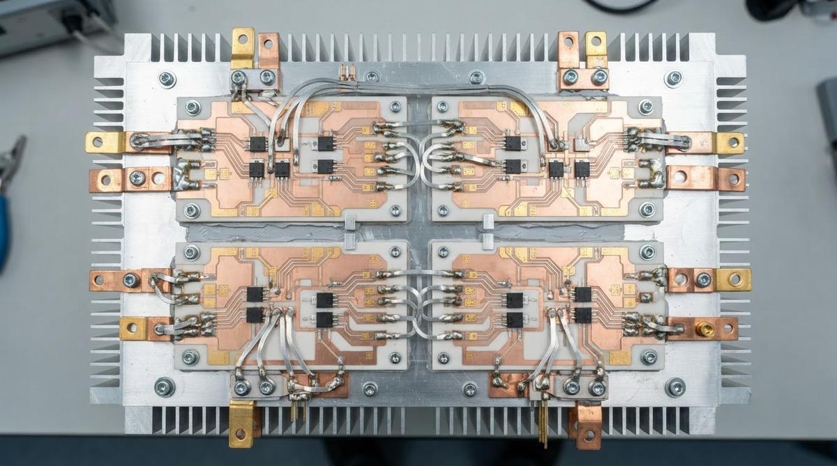
A DBC substrate with copper on one side only will bow after cooling from the bonding temperature. The mismatch in thermal contraction between copper and ceramic produces a concave warp on the copper side. For a 50 × 50 mm Al₂O₃ substrate with 0.3 mm copper on one face, bow can reach 50–100 µm—enough to cause solder voiding during module assembly.
The standard solution is to bond copper on both sides. The backside copper does not need to be patterned identically, but total copper area and thickness should be within 10–15% of the top side. If the backside is a plain ground plane, that often satisfies the balance requirement naturally. This is one of the most frequently overlooked DBC direct bonded copper layout guidelines, and ignoring it causes the most rework.
Substrate Material: Al₂O₃ vs. AlN for DBC
| Property | Al₂O₃ 96% | AlN | Unit | Condition | Source |
|---|---|---|---|---|---|
| Thermal conductivity | 24–28 | 170–200 | W/mK | 20 °C | CoorsTek, Kyocera datasheets |
| CTE | 7.0–7.4 | 4.5–4.8 | ppm/°C | 20–300 °C | CoorsTek, Kyocera datasheets |
| Flexural strength | 300–380 | 300–400 | MPa | ASTM C1161 | CeramTec, Kyocera datasheets |
| Dielectric strength | 10–15 | 14–17 | kV/mm | 25 °C, DC | CoorsTek datasheets |
| Relative cost | 1× | 3–5× | — | — | Industry pricing |
Typical values for commercially available material, for comparison only. Confirm against the datasheet for your specific grade.
AlN’s lower CTE is closer to silicon (2.6 ppm/°C) and SiC (4.0 ppm/°C), reducing die-attach fatigue. Choose AlN when junction temperatures exceed 150 °C or thermal resistance from die to heatsink is the binding constraint. Choose Al₂O₃ when cost matters more than thermal performance—it handles most applications below 100 W per die site.
When Not to Use DBC
DBC is the wrong process if your design needs fine-pitch traces below 0.3 mm. For signal routing with 50–100 µm lines, DPC or thin-film on ceramic are better fits. If your copper requirement is under 35 µm and the application is RF or sensor, LTCC co-fired ceramic or thin-film gives tighter tolerances and lower loss. For cost-sensitive, low-power applications, FR-4 or metal-core PCBs outperform DBC on price by an order of magnitude. DBC earns its cost in high-current, high-temperature, high-reliability power electronics—not general-purpose circuits.
Design Checklist Before Submitting DBC Artwork
- All copper features have corner radii ≥ copper thickness.
- Copper-to-edge clearance meets or exceeds 0.5 mm (adjust for scribe method).
- Top and bottom copper coverage is balanced within 15%.
- Creepage distances satisfy IEC 60664-1 for your working voltage.
- Die-attach pads are oversized by ≥0.5 mm per side.
- Wire-bond pads meet minimum size for your bond wire diameter.
- Isolation trenches are ≥0.5 mm wide for solder confinement.
- Fiducials and alignment marks are included if pick-and-place assembly is planned.
FAQ
Can I mix DBC with thin-film traces on the same substrate?
Yes, but it requires a two-step process: DBC bonding and etching first, then thin-film deposition and patterning on exposed ceramic areas. This adds cost and process complexity. It is used in some high-end power modules where both high current and fine signal routing are needed on one substrate.
What surface finishes work on DBC copper?
Bare copper (with oxide removal before assembly), electroless nickel/immersion gold (ENIG), and electrolytic nickel/gold are all common. For aluminum wire bonding, nickel/gold is standard. For solder die attach, bare copper or Ni/Au both work. Confirm finish thickness with your copper plating and finish supplier.
How many thermal cycles can a DBC substrate survive?
Reliability depends on copper thickness, substrate material, and cycle range. Published data from Kyocera and Rogers show that 0.3 mm Cu on Al₂O₃ typically survives 3,000–5,000 cycles of –40 °C to +125 °C before bond degradation. AlN substrates with the same copper can reach 2,000–4,000 cycles under the same conditions due to higher interfacial stress from AlN’s lower CTE. Wider temperature swings reduce cycle life sharply.
Is DBC the same as AMB (active metal brazing)?
No. DBC uses a copper-oxide eutectic bond formed at ~1070 °C, limited to Al₂O₃ and AlN. AMB uses a titanium-containing braze alloy at ~850 °C and can bond copper to Si₃N₄ as well. AMB produces a stronger bond and better thermal-cycle reliability on Si₃N₄, but costs more. For Al₂O₃ applications, DBC remains the more cost-effective choice.
Do I need to specify a backside copper pattern?
Yes. Even if the backside is unpatterned, specify full copper coverage for warpage control. If you leave the backside bare, expect measurable bow that complicates downstream soldering. Provide a backside Gerber or at minimum a note specifying full-area copper with the same thickness as the top side.