LTCC co-fired ceramic layout guidelines differ from standard PCB design in three critical ways: the green tape shrinks 12–16 % in X/Y during sintering, vias are punched before firing and must survive lamination pressure, and conductor pastes (silver, silver-palladium, gold) behave nothing like etched copper. Following proper LTCC co-fired ceramic layout guidelines from the start prevents open vias, cracked layers, and out-of-spec dimensions. The rules below give you the numbers you need to get a first-pass design through fabrication.
What Is LTCC and Why Layout Guidelines Matter
LTCC (Low-Temperature Co-Fired Ceramic) is a multilayer ceramic PCB technology in which unfired glass-ceramic tape layers are printed with conductor and resistor pastes, stacked, laminated, and co-fired at 850–900 °C. Because the entire structure sinters as one piece, every geometric feature on every layer must account for the same shrinkage factor. A mismatched shrinkage assumption between your CAD file and the tape manufacturer’s datasheet will shift every pad, via, and cavity edge proportionally.
LTCC tapes are typically alumina–glass composites (e.g., DuPont 951, Ferro A6M, Heraeus CT2000). Each tape system has its own shrinkage spec and compatible paste set. Confirm the exact tape you are designing for before committing any dimension. The values in this article are representative of common commercial LTCC systems; always cross-check against your supplier’s datasheet.
LTCC Co-Fired Ceramic Layout Guidelines for Conductor Trace and Space
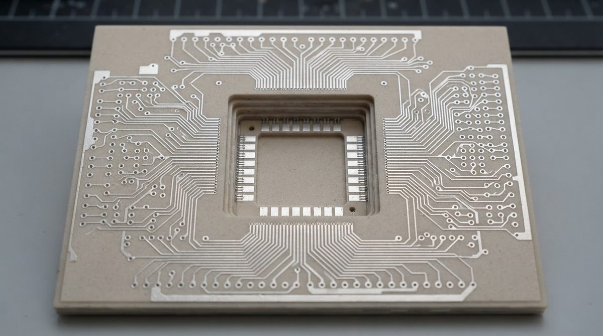
Conductors are screen-printed onto green tape, so resolution depends on mesh count, paste rheology, and squeegee pressure rather than photolithographic etch. Typical achievable values for production-grade LTCC:
| Parameter | Standard Process | Fine-Line Process | Unit | Notes |
|---|---|---|---|---|
| Min line width | 100–125 | 50–75 | µm | Post-fire dimension |
| Min space | 100–125 | 50–75 | µm | Post-fire dimension |
| Conductor thickness (fired) | 8–12 | 5–8 | µm | Silver or AgPd paste |
| Line width tolerance | ±15 | ±10 | µm | Within a single layer |
| Registration, layer-to-layer | ±25–50 | ±15–25 | µm | Depends on alignment method |
Typical values for commercially available LTCC systems. Confirm against the datasheet for your specific grade.
Design pads at least 75 µm larger than the via capture diameter on each side to absorb registration error. If you are accustomed to thick-film layout rules on pre-fired substrates, note that LTCC post-fire tolerances are looser because of shrinkage variation.
Via Design: Sizing, Pitch, and Fill
Vias in LTCC are punched or laser-drilled in the green tape, then filled with conductor paste before lamination. They are not plated. This means via diameter, fill quality, and keep-out spacing all follow different LTCC co-fired ceramic layout guidelines than FR-4 through-holes.
- Minimum via diameter (fired): 100–150 µm for standard punch; 50–80 µm for laser drill.
- Via pad diameter: Via diameter + 150–200 µm minimum (75–100 µm annular ring per side).
- Via-to-via pitch: ≥ 2× via diameter, center-to-center. Closer spacing risks punch-tool breakage and paste bridging.
- Via-to-edge clearance: ≥ 300 µm from any cavity wall or substrate edge to prevent cracking during lamination.
- Stacked vs. staggered vias: Stacked vias are possible in LTCC (unlike many organic PCBs) because the paste fills the full via barrel. Stacking more than 8–10 layers of vias may cause dimpling; stagger every 4–6 layers for structures above 10 layers.
Thermal Vias
To create a low-impedance thermal path, place thermal via arrays on a 400–500 µm pitch with 200 µm diameter vias. A 5 × 5 array of 200 µm stacked vias through a 10-layer LTCC stackup (total fired thickness ~1 mm) reduces thermal resistance by roughly 40–60 % compared to bare ceramic, depending on via fill density. Use the paste manufacturer’s thermal conductivity value (typically 200–250 W/mK for filled silver vias vs. 2–3 W/mK for the glass-ceramic tape) to run your own calculation.
Enter your substrate area, thickness, and via array parameters below to estimate the effective thermal resistance of your LTCC stackup with and without thermal vias.
Shrinkage Compensation: The Single Biggest Layout Mistake
LTCC green tape shrinks during sintering. A typical spec is 12.7 ± 0.3 % in X and Y, and 15 ± 1 % in Z, per the tape datasheet (e.g., DuPont 951 PDS). You must scale your CAD artwork by 1/(1 − shrinkage). For 12.7 % X/Y shrinkage, the scale factor is 1.1455. Getting this right is one of the most important LTCC co-fired ceramic layout guidelines to internalize.
Worked example: You need a 10.000 mm post-fire pad pitch. Pre-fire artwork dimension = 10.000 / (1 − 0.127) = 10.000 / 0.873 = 11.455 mm. If you use the wrong shrinkage value by just 0.5 % (12.2 % instead of 12.7 %), the post-fire pitch shifts to 10.000 × (1 − 0.122) / (1 − 0.127) = 10.057 mm. Over a 25 mm span, that becomes a 142 µm cumulative error, enough to misalign a BGA pad array.
Zero-shrinkage LTCC (e.g., Heraeus CT2000 with constraining layers) eliminates X/Y shrinkage but still shrinks in Z. If your design uses zero-shrinkage tape, do not apply X/Y scaling. Confirm which system your fabricator uses before generating artwork.
Cavity and Embedded Component Rules
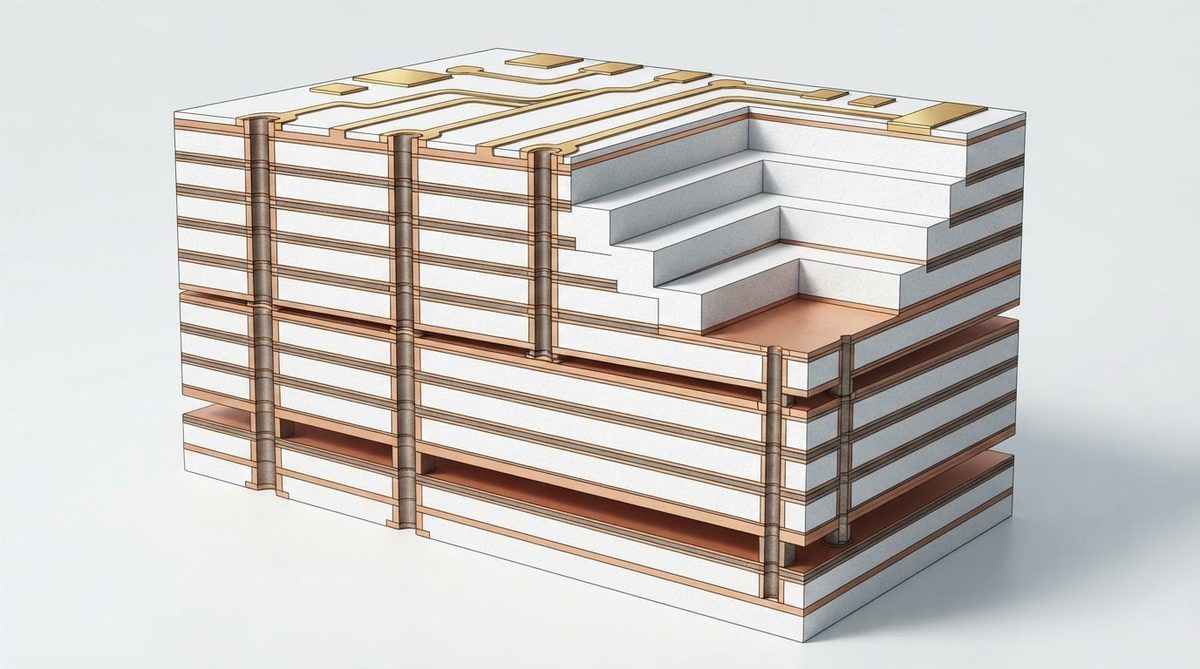
LTCC supports open cavities for die attach, sensor windows, and embedded passives. Cavity design is where most first-time designers applying LTCC co-fired ceramic layout guidelines run into yield problems.
- Minimum cavity wall thickness: 250–400 µm (fired) depending on cavity depth. Thinner walls crack during lamination.
- Cavity depth: Up to 70–80 % of total substrate thickness. Deeper cavities require stepped profiles to maintain wall integrity.
- Corner radii: Internal cavity corners must have a radius ≥ 200 µm. Sharp corners concentrate stress and initiate cracks during firing.
- Conductor routing near cavities: Keep traces ≥ 200 µm from cavity edges. Conductors at the cavity lip experience paste thinning during lamination.
Embedded resistors (e.g., ruthenium oxide paste) can be printed on internal layers and trimmed post-fire with laser. Allow ±20–30 % initial tolerance; laser trimming brings this to ±1–2 %. Place trim pads accessible from the top surface or cavity floor.
Layer Count and Stackup Considerations
Commercial LTCC stackups range from 2 to 60+ layers. Each green tape layer fires to roughly 90–110 µm thickness (tape-dependent). A 10-layer stackup fires to approximately 0.9–1.1 mm total thickness. Consider these rules:
- Assign ground and power planes to interior layers, signals to outer layers and cavity floors.
- Place ground planes adjacent to RF signal layers for controlled impedance. Stripline impedance in LTCC is achievable but requires tight dielectric constant control (εr typically 7.1–7.8 for alumina-glass tapes at 10 GHz, per DuPont 951 data).
- Avoid routing high-speed signals on the same layer as embedded resistors; resistor paste has different εr and loss tangent.
For designs requiring more than 20 layers, discuss warpage risk with your fabricator. Asymmetric conductor loading across the stackup causes differential shrinkage and bowing. Balance metal density across the Z-axis, or add dummy metallization on lightly loaded layers. These stackup-level LTCC co-fired ceramic layout guidelines are often overlooked until prototypes come back bowed.
When Not to Use LTCC
LTCC is the wrong choice if your design needs high current-carrying capacity (silver conductors are thin and resistive compared to thick copper on DBC or DPC substrates), if your production volume exceeds tens of thousands of units and cost per board matters more than RF performance, or if your operating temperature stays below 150 °C and FR-4 or standard MCPCB would suffice. For single-layer or two-layer designs without embedded passives, thin-film ceramic processes offer finer features at lower per-unit cost. LTCC shines in multilayer RF modules, hermetic sensor packages, and aerospace electronics where its combination of low loss tangent, embedded passives, and cavity capability cannot be matched by organic boards.
Frequently Asked Questions
Can I use standard Gerber files for LTCC?
Yes, most LTCC fabricators accept Gerber RS-274X or ODB++ files. You must apply the shrinkage scale factor in your CAD tool before generating output. Some fabricators prefer to apply scaling themselves from nominal-dimension files; confirm the workflow before submitting.
What paste systems are compatible with LTCC?
Silver (Ag), silver-palladium (AgPd), and gold (Au) conductor pastes are standard. Copper is not used because it oxidizes at LTCC firing temperatures (850–900 °C) in air. Each tape system has a qualified paste set from the tape manufacturer; mixing paste vendors without qualification risks delamination.
How many times can an LTCC substrate be re-fired?
Post-fire operations such as resistor trimming, brazing, or adding top-side thick-film conductors typically require 1–3 additional firings at lower temperatures (600–850 °C). Each re-fire risks additional shrinkage and conductor migration. Design for the minimum number of post-fire steps.
Is LTCC suitable for power electronics?
LTCC handles moderate power levels well, but its glass-ceramic body has low thermal conductivity (2–3 W/mK) compared to alumina (24–28 W/mK) or AlN (170–200 W/mK). For high-power applications above a few watts per square centimeter, consider thermal via arrays or switch to a higher-conductivity alumina LTCC substrate or a different technology entirely.
What is the typical lead time for an LTCC prototype?
Prototype LTCC runs generally take 3–6 weeks from approved artwork to shipped parts, depending on layer count and cavity complexity. This is longer than FR-4 quick-turn but comparable to other ceramic multilayer processes.
Do I need to account for camber or warpage in my layout?
Yes. LTCC substrates can exhibit camber of 2–5 mils per inch after firing, especially in high-layer-count or asymmetric stackups. Design solder pads with enough area to tolerate slight non-planarity, and specify camber limits in your procurement drawing per ASTM C1161 or your own internal standard.