A 50 Ω microstrip on 96% alumina (εr ≈ 9.4–9.9 at 10 GHz) needs a trace roughly 0.60 mm wide on a 0.635 mm substrate—about half the width you would use on FR-4. The microstrip alumina calculator and reference data on this page let you size traces for any alumina grade without guessing at material properties. Getting the number right matters because alumina’s high dielectric constant shrinks trace widths significantly, and a 5% error in εr shifts impedance by roughly 2–3 Ω.
Key Takeaways
- 96% alumina has a dielectric constant of 9.4–9.9 (1 MHz–10 GHz); 99.6% alumina runs 9.7–10.1 over the same range (per Kyocera and CoorsTek datasheets).
- Microstrip trace width on alumina is typically 40–55% narrower than the same impedance on FR-4 (εr ≈ 4.3–4.5).
- The Hammerstad–Jensen closed-form model matches full-wave simulation within ±1% for w/h ratios between 0.1 and 10.
- Loss tangent for 96% alumina is 0.0001–0.0004 at 10 GHz, making it practical for lines well above 40 GHz.
- Conductor loss usually dominates over dielectric loss on alumina; copper thickness and surface roughness matter more than εr tolerance for insertion loss.
Alumina Dielectric Properties for the Microstrip Alumina Calculator
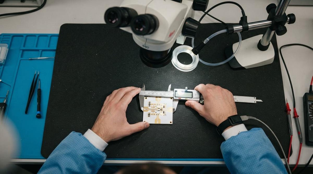
Impedance depends on three substrate parameters: dielectric constant (εr), substrate thickness (h), and loss tangent (tan δ). Alumina grades differ enough to change your trace width by 10–20 µm, so use the correct grade in any microstrip alumina calculator input.
| Parameter | 96% Al₂O₃ | 99.6% Al₂O₃ | Unit | Condition | Source |
|---|---|---|---|---|---|
| Dielectric constant (εr) | 9.4–9.9 | 9.7–10.1 | — | 1 MHz–10 GHz, 25 °C | Kyocera A-493, CoorsTek AD-96 |
| Loss tangent (tan δ) | 0.0001–0.0004 | 0.0001–0.0002 | — | 10 GHz, 25 °C | Kyocera A-493, CoorsTek AD-995 |
| Standard thickness (h) | 0.254, 0.381, 0.635, 1.016 | 0.254, 0.381, 0.635 | mm | As-fired tolerance ±1–2% | Industry standard |
| Surface roughness (Ra) | 0.3–0.8 | 0.05–0.25 | µm | As-fired / polished | CoorsTek datasheet |
Typical values for commercially available material, for comparison only. Confirm against the datasheet for your specific grade.
If you need a bare ceramic substrate in a non-standard thickness for your RF prototype, most suppliers can lap or grind alumina to custom dimensions with ±25 µm tolerance.
The Microstrip Impedance Equation on Alumina
The Hammerstad–Jensen model (IEEE Trans. MTT, 1980) is the standard closed-form approach used inside every microstrip alumina calculator. For a strip of width w on a substrate of height h with dielectric constant εr:
Effective dielectric constant:
ε_eff = (εr + 1)/2 + (εr − 1)/2 · (1 + 12·h/w)−0.5
Characteristic impedance (w/h ≤ 1):
Z₀ = (60 / √ε_eff) · ln(8h/w + w/4h)
Characteristic impedance (w/h > 1):
Z₀ = (120π / √ε_eff) / [w/h + 1.393 + 0.667·ln(w/h + 1.444)]
These equations assume zero-thickness conductors. For thick-film or DPC copper (typically 10–50 µm), apply a width correction: w_eff = w + (t/π)·[1 + ln(2h/t)], where t is the metal thickness.
Worked Example: 50 Ω on 96% Alumina, 0.635 mm Thick
Target: Z₀ = 50 Ω. Substrate: 96% Al₂O₃, h = 0.635 mm, εr = 9.6 (mid-range). Copper: 10 µm thick-film. Walk through this by hand, then verify with the microstrip alumina calculator below.
- Initial guess. For εr ≈ 9.6 and 50 Ω, w/h is roughly 0.37 (from published design charts, e.g., Pozar, Microwave Engineering, Table 3.3). So w ≈ 0.37 × 0.635 = 0.235 mm.
- Compute ε_eff. ε_eff = (9.6 + 1)/2 + (9.6 − 1)/2 · (1 + 12/0.37)−0.5 = 5.30 + 4.30 · 0.168 = 6.02.
- Compute Z₀ (w/h < 1 path). Z₀ = (60 / √6.02) · ln(8/0.37 + 0.37/4) = 24.47 · ln(21.72) = 24.47 × 3.078 = 75.3 Ω. Too high—iterate.
- Iterate. Increase w/h to 0.95. ε_eff = 5.30 + 4.30 · (1 + 12/0.95)−0.5 = 5.30 + 4.30 · 0.270 = 6.46. Z₀ = (60/√6.46) · ln(8/0.95 + 0.95/4) = 23.61 · ln(8.66) = 23.61 × 2.159 = 50.97 Ω. Close enough for a first pass.
- Result. w = 0.95 × 0.635 = 0.603 mm. Apply the thickness correction for 10 µm copper: w_eff ≈ 0.603 + 0.006 = 0.609 mm.
A 50 Ω line on 0.635 mm 96% alumina is about 0.60 mm wide. On FR-4 at the same thickness it would be roughly 1.15 mm. That 48% reduction is why alumina is favored for compact RF circuits.
Enter your own substrate thickness, εr, and target impedance into the microstrip alumina calculator to get a result instantly:
[pcb_calc type=”microstrip-impedance”]
How εr Tolerance Affects Impedance
Alumina εr can vary ±3% lot-to-lot. For the 50 Ω line above, shifting εr from 9.6 to 9.9 changes ε_eff from 6.46 to 6.63, which drops Z₀ from 51.0 Ω to about 49.5 Ω. That is a 1.5 Ω swing—usually acceptable for 50 Ω designs but potentially problematic for tightly specified filters or couplers at millimeter-wave frequencies.
If your design cannot tolerate ±1.5 Ω, consider specifying a tighter εr lot from your substrate vendor, or move to 99.6% alumina, which has a narrower εr spread (±1.5% typical). The trade-off is cost: 96% alumina substrates run roughly half the price of 99.6% grade in small volumes.
Conductor Loss vs. Dielectric Loss on Alumina
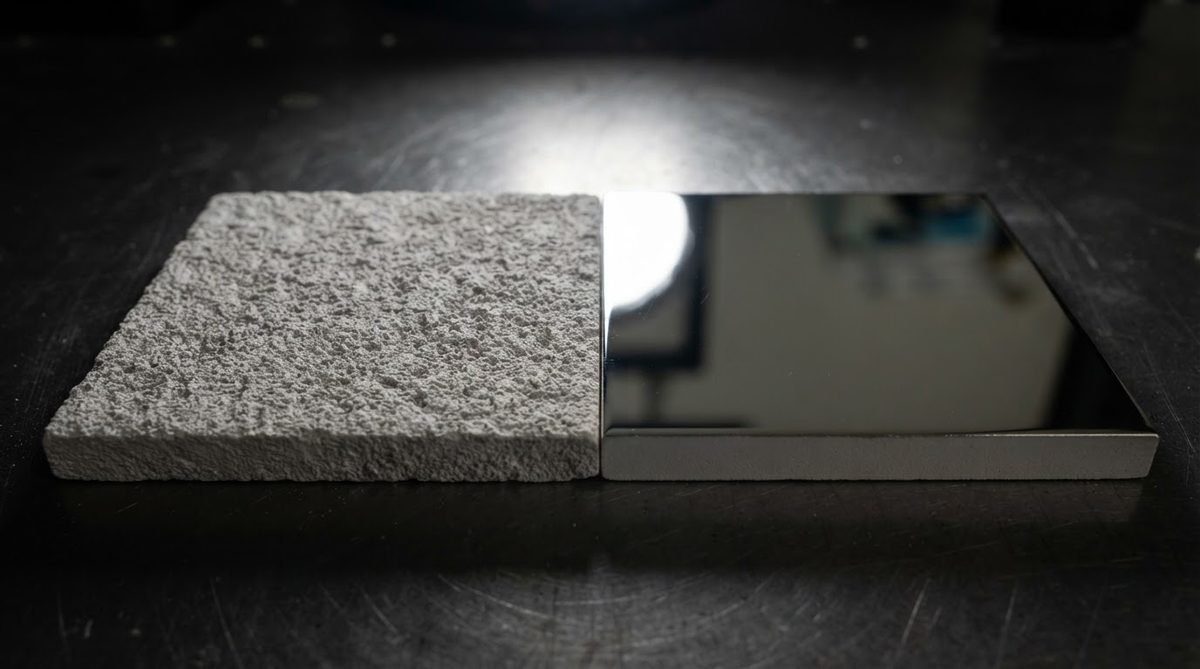
At 10 GHz on a 0.635 mm 96% alumina substrate with 10 µm copper, conductor loss is approximately 0.15–0.25 dB/cm while dielectric loss is only 0.01–0.02 dB/cm (calculated per the methods in Pozar, Microwave Engineering, 4th ed., Chapter 3). Conductor loss dominates by 10×.
Practical implication: spending money on 99.6% alumina (lower tan δ) yields minimal insertion-loss improvement unless you are above 30 GHz. Below that, invest in smoother substrates and thicker copper instead. A polished 96% alumina substrate with Ra < 0.2 µm can cut conductor loss by 15–20% compared to an as-fired surface. For copper-metallized alumina boards, specify polished substrates and electroplated copper for best RF performance.
When Not to Use Alumina for Microstrip
Alumina is the default RF substrate up to about 40 GHz, but it is not always the right choice:
- Cost-sensitive, below 6 GHz. Rogers RO4003C (εr ≈ 3.55) or similar PTFE laminates are cheaper, easier to machine, and adequate for most sub-6 GHz designs.
- Large panel sizes. Alumina substrates are typically limited to about 100 × 100 mm (some vendors go to 150 × 150 mm). If your circuit exceeds that, you need a laminate or a tiled approach with wire bonds.
- Tight mechanical shock requirements. Alumina is brittle. A board subject to repeated mechanical shock or vibration may crack. Consider AlN (higher fracture toughness) or a hybrid approach with an alumina RF section bonded to a metal carrier.
- Very high thermal loads. If your substrate also serves as the primary heat spreader and you need >100 W/cm² dissipation, alumina’s 24–28 W/mK thermal conductivity may not be enough. Aluminum nitride (170–200 W/mK) is the usual step up.
Frequently Asked Questions
What dielectric constant should I use for 96% alumina at 10 GHz?
Use 9.4–9.9, with 9.6 as a reasonable mid-point for initial design. The exact value depends on the manufacturer and lot. Kyocera’s A-493 datasheet specifies 9.8 at 1 MHz; values drop slightly with frequency. Always request the vendor’s measured εr data for your specific substrate lot if your impedance tolerance is below ±2 Ω.
Can I get 50 Ω microstrip on a 0.254 mm alumina substrate?
Yes, but the trace will be very narrow—roughly 0.24 mm wide—which pushes the limits of thick-film screen printing (typically ±25 µm). Thin-film or DPC metallization, with ±5–10 µm capability, is a better process choice for thin substrates. Confirm your manufacturer’s minimum trace width before committing to a thin substrate.
Does alumina’s dielectric constant change with temperature?
It does, but the shift is small. The temperature coefficient of εr for 96% alumina is approximately +100 to +150 ppm/°C (per CoorsTek AD-96 data). Over a 100 °C rise, εr increases by about 1–1.5%, shifting a 50 Ω line by roughly 0.3–0.4 Ω. For most applications this is negligible.
How does surface roughness affect my microstrip impedance?
Surface roughness does not significantly change impedance, but it increases conductor loss. The Hammerstad roughness correction factor shows that Ra = 0.8 µm (typical as-fired 96% alumina) adds roughly 10–15% to conductor loss at 10 GHz compared to a perfectly smooth surface. Polishing to Ra < 0.2 µm recovers most of that loss.
Is alumina better than quartz for microstrip at millimeter-wave?
Fused quartz (εr ≈ 3.8, tan δ ≈ 0.0001) offers lower dielectric loss than alumina above 40 GHz and wider traces for a given impedance, simplifying fabrication. Alumina’s advantage is higher εr for circuit miniaturization and better thermal performance for power-dissipating circuits. Choose quartz for low-loss receive paths; choose alumina when size or thermal management matters more.
Next Step
If you have a target impedance and substrate thickness in mind, run the microstrip alumina calculator above to get your trace width, then export the result into your EM simulator for verification. When you are ready to source substrates or metallized boards, review the ceramic PCB manufacturing process to decide between thick-film, thin-film, and DPC metallization for your frequency range.