Ceramic PCB testing combines visual, dimensional, electrical, thermal, and mechanical screens applied in a defined sequence — from incoming substrate inspection through final outgoing quality checks. The goal is to confirm that every board meets its datasheet claims before it ships, because ceramic substrates serve applications (power electronics, RF, medical implants, aerospace) where a field failure is unacceptable.
Key Takeaways
- A typical ceramic PCB test flow includes 7–10 discrete inspection or test steps, from raw substrate through packaged board.
- Thermal cycling per IPC-9701 or JESD22-A104 is the single most revealing reliability screen for ceramic boards, exposing CTE-mismatch failures that visual inspection cannot catch.
- Hipot (dielectric withstand) testing at 2–5 kV AC for 60 s is standard for high-voltage ceramic boards; breakdown voltages for 96% Al₂O₃ exceed 10 kV/mm per ASTM D149.
- Copper peel strength on DBC substrates typically ranges from 1.0–1.8 kgf/cm, measured per IPC-TM-650 2.4.8.
- First article inspection (FAI) per AS9102 is required for aerospace and defense ceramic PCB orders and should be requested for any safety-critical application.
Why Ceramic PCBs Need a Dedicated Test Sequence
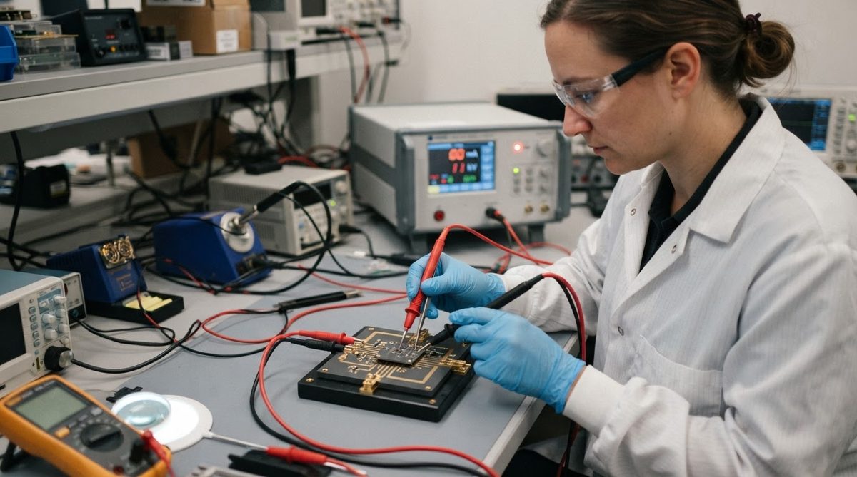
FR-4 boards flex. Ceramic boards do not. That brittleness means defects that would be cosmetic on an organic laminate — a hairline crack, a subsurface void, a marginally weak copper bond — can propagate under thermal or mechanical stress and cause catastrophic open circuits. Standard IPC Class 2 acceptance criteria written for organic boards are often insufficient. Most ceramic PCB specs reference IPC-6012 for general requirements and layer on material-specific tests drawn from ASTM, JEDEC, and MIL-STD-883.
The test sequence also matters because ceramic substrates are expensive. Catching a bad lot at incoming inspection costs far less than discovering it after die attach. A well-structured test plan gates each process step so that defective units are removed early, which directly improves yield and scrap rate.
The Full Ceramic PCB Test Flow
The table below shows a representative test sequence for a DBC or DPC ceramic PCB. Not every board needs every test — the right subset depends on the application, the customer’s quality spec, and whether the board is a prototype or production unit.
| Step | Test / Inspection | Method / Standard | Typical Criteria | When Applied |
|---|---|---|---|---|
| 1 | Incoming substrate inspection | Visual + dimensional (caliper, CMM) | No cracks, chips > 0.1 mm; thickness ± 0.025 mm | Raw substrate receipt |
| 2 | Surface roughness check | Profilometer, Ra per ASME B46.1 | Ra 0.3–0.8 µm (as-fired Al₂O₃ 96%) | Before metallization |
| 3 | Post-metallization visual / AOI | Automated optical inspection | No opens, shorts, trace width ± 10% | After copper patterning |
| 4 | Dimensional / registration | CMM or optical comparator | Feature position ± 0.05 mm typical | After patterning |
| 5 | Copper peel strength | IPC-TM-650 2.4.8 | ≥ 1.0 kgf/cm (DBC); ≥ 0.6 kgf/cm (DPC thin film) | Sample destructive |
| 6 | Hipot / dielectric withstand | IEC 60243-1, ASTM D149 | No breakdown at 2–5 kV AC, 60 s | 100% or sample |
| 7 | Continuity / isolation | Flying probe or bed-of-nails | Continuity < 10 Ω; isolation > 100 MΩ at 500 V DC | 100% |
| 8 | Solderability | IPC J-STD-003, dip-and-look | ≥ 95% wetting within 5 s | Sample per lot |
| 9 | Thermal cycling | JESD22-A104 or IPC-9701 | No delamination or cracking after 500–1000 cycles (−40 °C to +125 °C) | Qualification / periodic |
| 10 | Flexural strength (3-point bend) | ASTM C1161 | ≥ 300 MPa (Al₂O₃ 96%) | Sample destructive |
Typical values for commercially available material, for comparison only. Confirm against the datasheet for your specific grade.
Electrical Testing: Hipot and Isolation
The hipot test on ceramic substrates applies a high AC or DC voltage between conductors (or between a conductor and the substrate backside) and checks for current leakage or dielectric breakdown. For 96% alumina at 0.635 mm thickness, the theoretical breakdown voltage exceeds 6 kV based on a dielectric strength of roughly 10–15 kV/mm (per ASTM D149 at 60 Hz, 20 °C). In practice, production hipot is run at 2–5 kV AC for 60 seconds with a leakage limit of 1–5 mA, depending on the customer spec.
Continuity and isolation tests follow. Flying-probe testers verify every net for continuity (typically < 10 Ω) and check adjacent nets for isolation (> 100 MΩ at 500 V DC). These are 100% tests on production boards — no sampling.
Mechanical Testing: Peel Strength and Flexure
Copper peel strength is the single best predictor of long-term metallization reliability on a ceramic substrate. The test per IPC-TM-650 2.4.8 pulls a 1 mm-wide copper strip at 90° and records the force per unit width. DBC (direct bond copper) on Al₂O₃ typically yields 1.0–1.8 kgf/cm. Thin-film DPC processes yield 0.5–0.8 kgf/cm. AMB (active metal brazing) on Si₃N₄ can exceed 2.0 kgf/cm.
Three-point bend testing per ASTM C1161 measures the substrate’s flexural strength. This is a destructive test run on sample coupons, not production boards. It matters most for substrates that will see mechanical shock or vibration — automotive under-hood modules, for example.
Thermal Cycling: The Most Revealing Reliability Screen
Thermal cycling reliability testing subjects assembled or bare boards to repeated temperature swings, typically −40 °C to +125 °C (or −55 °C to +150 °C for military). The CTE mismatch between copper (~17 ppm/°C) and alumina (~7 ppm/°C) generates shear stress at the bond interface on every cycle. After 500–1000 cycles, the boards are cross-sectioned and inspected for crack initiation, delamination, or resistance drift.
A worked example: a DBC board with 0.3 mm copper on 0.635 mm Al₂O₃ 96% cycling from −40 °C to +125 °C experiences a ΔT of 165 °C. The differential thermal strain is approximately (17 − 7) × 10⁻⁶ × 165 = 1.65 × 10⁻³, or 0.165%. Over a 20 mm copper island, that translates to ~3.3 µm of differential displacement per cycle at the edge. Multiply by 1000 cycles, and the cumulative fatigue loading becomes the dominant failure mechanism. This is why copper island size and edge geometry matter as much as material choice.
Solderability and Surface Finish Verification
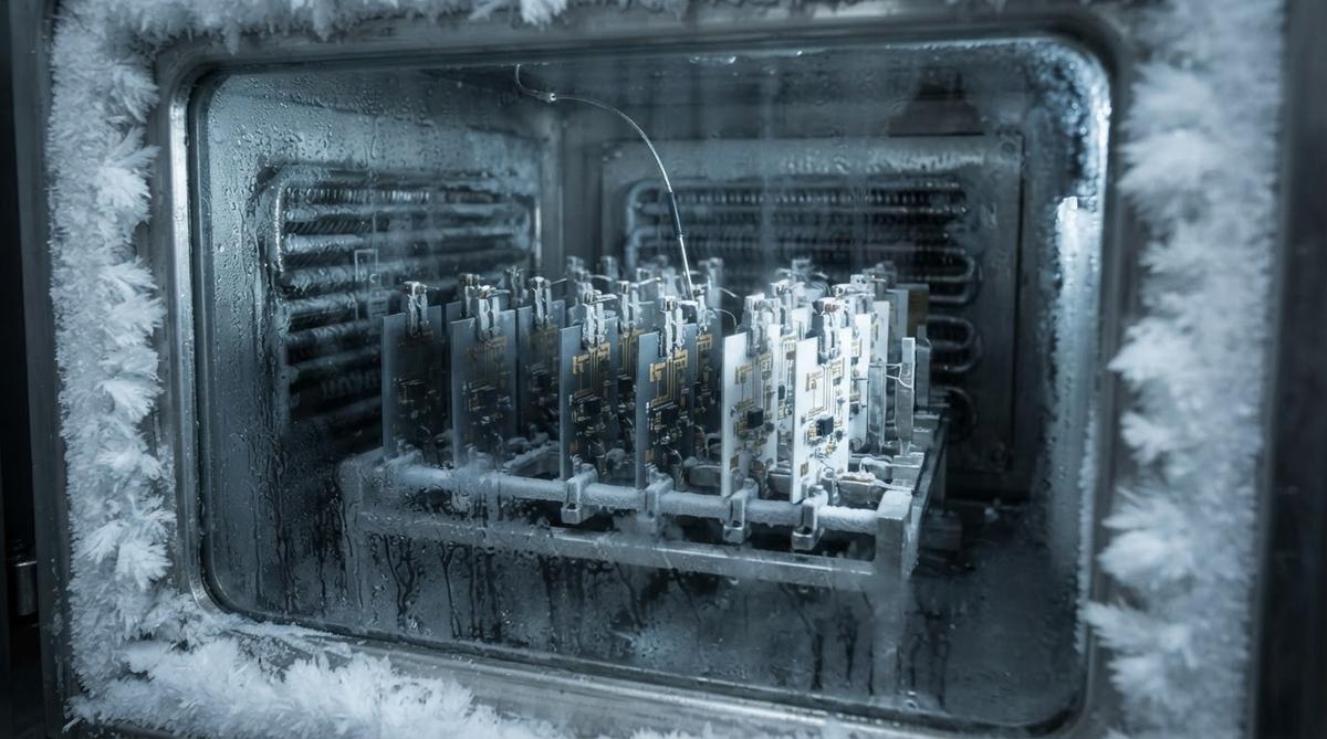
Solderability screening per IPC J-STD-003 uses a dip-and-look method: pads are fluxed, dipped in molten solder (typically SAC305 at 245 °C for 5 s), and examined for wetting coverage. The acceptance threshold is ≥ 95% wetting. Ceramic boards with ENIG or ENEPIG finishes generally pass easily. Bare copper pads that have oxidized during storage may not, which is why shelf-life limits and vacuum-sealed packaging matter.
First Article Inspection and Traceability
For aerospace and defense programs, first article inspection per AS9102 documents every critical dimension, material certification, and test result for the first production unit. Even outside aerospace, requesting FAI on a ceramic PCB order gives you a baseline record that simplifies root-cause analysis if failures appear later.
Lot-level traceability — linking each board to its substrate lot, metallization batch, and test data — is standard practice for medical and automotive ceramic boards. It enables targeted recalls and trend analysis across production runs.
When NOT to Use the Full Test Battery
Running every test in the table above on every board is neither practical nor cost-effective for all applications. If your ceramic PCB is a low-voltage LED submount operating at room temperature with no safety certification requirement, 100% AOI plus 100% electrical test plus sample solderability is likely sufficient. Skip thermal cycling qualification if the board never sees more than a 60 °C swing in service. Skip flexural testing if the board is bonded to a rigid heatsink and will never experience mechanical shock.
Conversely, if you are designing for implantable medical devices, automotive AEC-Q qualification, or space-grade hardware, the full battery — plus additional screens like HALT (highly accelerated life test), partial discharge testing, or hermeticity checks — is the minimum. The cost of testing is trivial compared to the cost of a field failure in these applications.
Frequently Asked Questions
Is 100% hipot testing standard for ceramic PCBs?
Yes, for boards rated above 500 V or used in safety-critical applications. Lower-voltage boards may use sample-based hipot per the customer’s quality plan. The test voltage is typically 2× the rated working voltage plus 1000 V, applied for 60 seconds.
How many thermal cycles should I specify for qualification?
500 cycles at −40 °C to +125 °C is a common baseline per JESD22-A104 Condition G. Automotive and aerospace programs often require 1000 cycles or more. The right number depends on the expected service life and the thermal excursion the board will see in the field.
Can I test ceramic PCBs on a standard flying-probe tester?
Yes. Standard flying-probe testers work on ceramic boards, but probe pressure settings may need adjustment to avoid cracking thin substrates (≤ 0.25 mm). Fixtureless testing is preferred for prototypes; bed-of-nails fixtures are more efficient for production volumes above a few hundred pieces.
Does copper peel strength degrade after thermal cycling?
It can. A 10–20% reduction in peel strength after 1000 thermal cycles (−40 °C to +125 °C) is typical for DBC on alumina. If post-cycling peel strength drops below 0.8 kgf/cm, the metallization process or copper island geometry should be reviewed.
What test standards apply specifically to ceramic substrates?
ASTM C1161 covers flexural strength. ASTM D149 and IEC 60243-1 cover dielectric strength. IPC-TM-650 covers peel strength and other PCB-level tests. JEDEC JESD22-A104 covers thermal cycling. MIL-STD-883 applies to military hybrid microcircuits on ceramic. There is no single unified standard for ceramic PCB testing; the test plan is assembled from these sources based on the application.
Next Step
If you are defining a test plan for a ceramic PCB project, start by identifying which screens from the table above apply to your application class. For a detailed discussion of any individual test, see the ceramic PCB FAQ. When you are ready to discuss test requirements alongside your board design, request a quote and include your quality spec or test plan in the upload.