A dielectric withstand test—commonly called a hipot test—applies a voltage well above the circuit’s rated working voltage across the insulation of a ceramic PCB and checks for breakdown or excessive leakage current. For most ceramic substrates (Al₂O₃ 96%, AlN, Si₃N₄), the bulk dielectric strength ranges from 10 to 25 kV/mm, so the substrate itself rarely fails. The weak points are edges, vias, surface contamination, and thin metallisation gaps. A properly designed hipot test catches those defects before they reach the field.
Key Takeaways
- Standard hipot test voltage is typically 2× rated voltage + 1 000 V (AC) or the DC equivalent at 1.414× the AC value, per IEC 60664-1 and IPC-9201.
- 96% alumina has a dielectric strength of 10–15 kV/mm (ASTM D149); AlN is 15–17 kV/mm; Si₃N₄ is 15–20 kV/mm.
- Leakage current trip limits for ceramic PCBs are usually set at 1–5 mA for AC hipot and 0.5–2 mA for DC hipot.
- Dwell time is 60 s for production per IEC 60664-1, though some automotive specs require 5 s at elevated voltage.
- Most hipot failures on ceramic boards trace to surface flashover or via defects, not bulk substrate breakdown.
What Is a Dielectric Withstand Test?
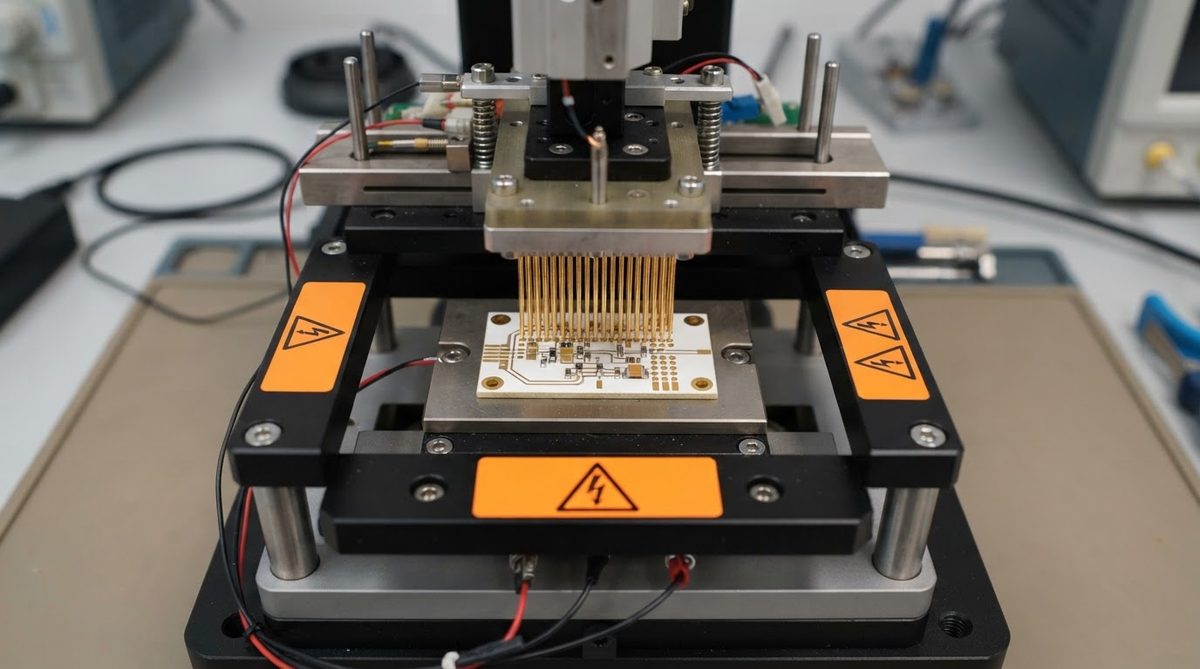
A dielectric withstand test is a pass/fail screen that proves an insulation barrier can handle a specified overvoltage without arcing, tracking, or excessive leakage. The test equipment—a hipot tester—ramps voltage between two conductors (or between a conductor and a ground plane) while monitoring leakage current. If current stays below the trip threshold for the full dwell period, the board passes.
This test is distinct from insulation resistance (IR) testing, which measures megohm-level resistance at low voltages (typically 500 V DC). IR testing finds gross contamination; hipot testing stresses the dielectric under field-realistic transients. Both are part of a complete ceramic PCB reliability screening program.
How to Choose the Test Voltage
The test voltage depends on the rated working voltage, the applicable safety standard, and the insulation class. The most common formula comes from IEC 60664-1:
AC hipot voltage = 2 × Vrated + 1 000 V
DC hipot voltage = (2 × Vrated + 1 000 V) × 1.414
For a power module rated at 600 V DC, the AC hipot voltage would be 2 × 600 + 1 000 = 2 200 V AC. The DC equivalent is 2 200 × 1.414 ≈ 3 111 V DC. Some standards (UL 60950, IEC 62368-1) specify different multipliers or add altitude derating. Always confirm the exact requirement in your end-product safety standard.
Worked Example: 1 200 V SiC Half-Bridge on AlN DBC
Rated working voltage: 1 200 V DC. Per IEC 60664-1, AC hipot = 2 × 1 200 + 1 000 = 3 400 V AC (rms), applied for 60 s. The AlN substrate is 0.635 mm thick with a dielectric strength of 15–17 kV/mm. Theoretical breakdown voltage of the bulk ceramic: 0.635 × 15 000 = 9 525 V minimum. The 3 400 V test stresses the substrate to roughly 36% of its minimum bulk strength—a comfortable margin. The real risk is at metallisation edges where field concentration can double the local stress.
Enter your rated voltage, substrate material, and thickness below to calculate the recommended hipot test voltage and compare it against the substrate’s theoretical breakdown margin.
[pcb_calc type=”hipot-test”]
Test Procedure Step by Step
- Fixture the board. Place the DUT on a grounded conductive plate or use spring-loaded probes to contact the specific nets under test. Ensure no operator can touch live conductors—hipot voltages are lethal.
- Set parameters. Program voltage, ramp rate (typically 100–500 V/s), dwell time (60 s standard, 5 s for 100% production screening at higher voltage per some automotive specs), and leakage trip limit.
- Ramp up. The tester increases voltage linearly. A sudden ramp can cause capacitive current spikes that trigger false failures, especially on multilayer ceramic PCB builds with large internal ground planes.
- Dwell. Hold at test voltage for the full dwell period. Monitor leakage current continuously.
- Ramp down. Reduce voltage gradually. Do not disconnect under load—stored charge in the ceramic’s bulk capacitance can arc during abrupt disconnection.
- Record results. Log peak leakage, pass/fail, serial number, and date. This data feeds into lot traceability and serialisation records.
Dielectric Strength of Common Ceramic Substrates
| Material | Dielectric Strength (kV/mm) | Typical Substrate Thickness (mm) | Approx. Breakdown Voltage (kV) | Test Standard | Source |
|---|---|---|---|---|---|
| Al₂O₃ 96% | 10–15 | 0.635 | 6.4–9.5 | ASTM D149 | CoorsTek ADS-96R datasheet |
| Al₂O₃ 99.6% | 12–16 | 0.635 | 7.6–10.2 | ASTM D149 | Kyocera A-493 datasheet |
| AlN | 15–17 | 0.635 | 9.5–10.8 | ASTM D149 | Maruwa AlN datasheet |
| Si₃N₄ | 15–20 | 0.32 | 4.8–6.4 | ASTM D149 | Kyocera SN-282 datasheet |
Typical values for commercially available material, for comparison only. Confirm against the datasheet for your specific grade.
Note that Si₃N₄ substrates are often thinner (0.32 mm) for mechanical toughness reasons, which reduces the absolute breakdown voltage despite a high per-millimetre strength. This matters when specifying hipot voltage for thin substrates.
Common Failure Modes on Ceramic PCBs
Surface Flashover
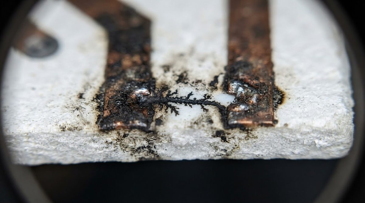
The most frequent hipot failure on ceramic boards is not through the bulk ceramic but across its surface. Contamination—flux residue, fingerprint oils, humidity films—creates a conductive path between traces. Cleaning with isopropyl alcohol and controlling ambient humidity below 60% RH during test eliminates most surface flashover events.
Via and Through-Hole Defects
Unfilled or partially metallised vias can trap air pockets. Air breaks down at roughly 3 kV/mm—far below the ceramic’s own strength. X-ray inspection of vias before hipot testing catches voids that would otherwise cause field failures.
Edge Chipping
Micro-cracks at laser-scribed or mechanically snapped edges reduce the effective insulation distance. For high-voltage boards, specify a minimum edge-to-conductor clearance of 0.5 mm or more, and inspect edges at 10× magnification.
AC vs DC Hipot: Which to Use
AC hipot stresses both polarities of the dielectric every cycle and is the default for safety certification (IEC 60664-1, UL standards). DC hipot is preferred for production screening of ceramic substrates because it generates lower capacitive charging current, reducing false failures on high-capacitance multilayer boards. DC also avoids repeated polarity reversal that can degrade thin-film metallisation over thousands of test cycles in high-volume production.
If your safety standard mandates AC, use AC. If you have a choice for production screening, DC at 1.414× the AC value gives equivalent stress with fewer nuisance trips.
When NOT to Use a Hipot Test
Hipot testing is not always appropriate or sufficient:
- Boards with sensitive active components already mounted. Hipot voltage can destroy ESD-sensitive ICs. Test bare boards or substrates before assembly, or use partial discharge testing at lower voltages.
- Very thin substrates (≤ 0.25 mm). The theoretical breakdown margin may be too thin for a standard 2× + 1 000 V test. Calculate the margin first; if it is below 3×, consult your safety engineer about reduced test voltage or partial discharge testing per IEC 60270.
- Low-voltage signal boards (≤ 50 V). Insulation resistance testing at 500 V DC per IPC-9201 is usually sufficient and faster. A full hipot adds cost without meaningful additional screening value.
- Repeated testing on the same unit. Each hipot cycle degrades the dielectric slightly. Limit production hipot to one or two applications per board. If retesting is needed after rework, document the cumulative exposure.
Applicable Standards
| Standard | Scope | Key Requirement |
|---|---|---|
| IEC 60664-1 | Insulation coordination for low-voltage equipment | Defines test voltage vs. working voltage, pollution degree, altitude |
| IPC-9201 | Surface insulation resistance (SIR) handbook | IR and hipot guidance for PCBs |
| IEC 60270 | Partial discharge measurements | Used when hipot alone cannot detect incipient breakdown |
| UL 60950-1 / IEC 62368-1 | IT/AV equipment safety | Specifies hipot voltage by insulation class (basic, supplementary, reinforced) |
| AEC-Q200 (passive) | Automotive passive component qualification | Dielectric withstand at 2.5× rated voltage for 60 s |
Relationship to Other Reliability Tests
Hipot testing is one element of a broader qualification sequence. Boards that pass hipot at room temperature may fail after thermal cycling reliability exposure if CTE mismatch opens micro-cracks in metallisation or vias. A robust qualification plan runs hipot both before and after environmental stress—typically after 500 or 1 000 thermal cycles per the relevant JEDEC or AEC-Q standard. Combining hipot with solderability verification and visual inspection after environmental exposure gives a complete picture of insulation integrity.
FAQ
Can a ceramic PCB fail hipot even though ceramics are great insulators?
Yes. Bulk ceramic rarely fails, but surface contamination, via voids, and edge cracks create weak paths that arc well below the substrate’s intrinsic dielectric strength. Most hipot failures on ceramic boards are surface or defect-driven, not bulk failures.
Does hipot testing damage the board?
A single properly conducted hipot test at the correct voltage does not measurably degrade a defect-free ceramic substrate. Repeated testing or excessive voltage can cause cumulative dielectric degradation. Limit production hipot to one application per board when possible.
What leakage current limit should I set for a ceramic PCB hipot test?
For AC hipot, 1–5 mA is typical; for DC hipot, 0.5–2 mA. The exact limit depends on board area, capacitance, and humidity. Start with the lower value and adjust upward only if you see consistent nuisance trips on known-good boards.
Should I hipot test before or after soldering components?
Test the bare substrate or metallised board before component assembly. Active components, especially MOSFETs and ICs, can be destroyed by hipot voltage. If post-assembly testing is required by your safety standard, use partial discharge testing or a reduced voltage with appropriate safeguards.
How does altitude affect the required hipot voltage?
IEC 60664-1 requires voltage derating above 2 000 m altitude because air’s dielectric strength decreases with pressure. At 5 000 m, the required clearance distances roughly double compared to sea level. If your product operates at altitude, apply the correction factors from IEC 60664-1 Table F.4 to both the working voltage rating and the hipot test voltage.
Next Step
If you need ceramic substrates qualified to a specific hipot voltage, include the test voltage, dwell time, and leakage limit in your procurement spec. For a quote on boards with hipot-tested deliverables, submit your files at AluminaPCB.com and specify the dielectric withstand requirement in the notes field.