Thermal cycling reliability ceramic substrates deliver is substantial: 96% alumina routinely survives 3,000–10,000+ cycles at –55 °C to +150 °C before first failure, while standard FR-4 typically fails at 500–1,500 cycles and aluminum-core MCPCB at 800–2,000 cycles under the same profile. The dominant reason is coefficient of thermal expansion (CTE) match. 96% alumina sits at 6.5–7.2 ppm/°C, close to silicon’s 2.6 ppm/°C and GaN’s 3.2 ppm/°C, so solder joints between die and substrate see far less strain per cycle than joints on FR-4 (14–17 ppm/°C) or MCPCB dielectric layers (typically 10–14 ppm/°C in-plane).
Key Takeaways
- 96% alumina ceramic PCBs endure 3,000–10,000+ cycles (–55 °C to +150 °C, per IEC 60068-2-14 Na) before solder-joint or metallization failure.
- FR-4 boards commonly show barrel cracking and pad lift between 500 and 1,500 cycles under the same profile.
- CTE mismatch is the primary driver of solder-joint fatigue; ceramic’s low CTE (6.5–8.5 ppm/°C depending on grade) keeps strain amplitudes small.
- Ceramic substrates cannot delaminate because they are monolithic; FR-4 and MCPCB dielectric layers can separate under thermal stress.
- The Coffin–Manson relation lets you estimate cycle-life differences quantitatively when you know the strain range.
Why CTE Mismatch Drives Thermal Cycling Reliability in Ceramic Assemblies
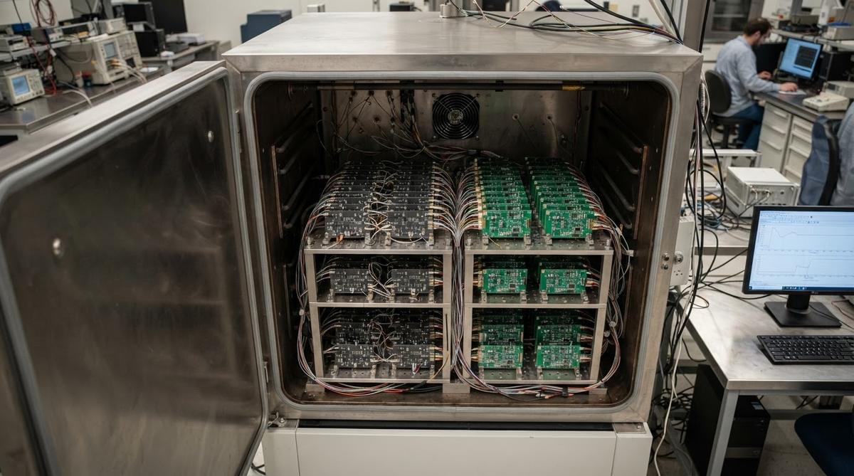
Every temperature swing forces bonded materials with different CTEs to expand and contract by different amounts. The resulting shear strain concentrates at solder joints, wire bonds, and interfaces between substrate layers. Over hundreds or thousands of cycles, this strain nucleates fatigue cracks in solder, eventually causing open circuits or increased thermal resistance at the die attach.
The Coffin–Manson relation describes this fatigue life:
Nf = C · (Δε)−n
where Nf is cycles to failure, Δε is the inelastic strain range per cycle, and C and n are material constants (n ≈ 1.9–2.5 for SAC305 solder, per Engelmaier’s modified model). Because Δε is roughly proportional to the CTE difference between substrate and component, halving the CTE mismatch can increase cycle life by a factor of 3.6–5.7×. This relationship is central to understanding thermal cycling reliability ceramic boards achieve versus organic alternatives.
Worked Example: Solder Joint Life Estimate
Assume a 5 mm × 5 mm silicon die (CTE 2.6 ppm/°C) soldered to three substrates with SAC305 (n = 2.0 for simplicity), ΔT = 200 °C (–55 °C to +145 °C), solder joint height 75 µm, and die-to-neutral-point distance 3.5 mm.
Shear strain γ ≈ (ΔCTE × ΔT × L) / h, where L is the distance to neutral point and h is joint height.
| Substrate | CTE (ppm/°C) | ΔCTE vs Si | γ (shear strain) | Relative Nf (Coffin–Manson, n=2) |
|---|---|---|---|---|
| 96% Al₂O₃ ceramic | 6.8 | 4.2 | 0.0392 | 1.0× (baseline) |
| FR-4 | 14.0 | 11.4 | 0.1064 | 0.14× (~7× fewer cycles) |
| MCPCB (Al core, dielectric layer) | 12.0 | 9.4 | 0.0878 | 0.20× (~5× fewer cycles) |
Illustrative calculation using simplified Coffin–Manson with n = 2. Real joint geometry, creep, and dwell time shift absolute numbers. Use for relative comparison only.
This means that if the ceramic assembly lasts 5,000 cycles, the same die on FR-4 would fail near 700 cycles and on MCPCB near 1,000 cycles, all else being equal. The strain reduction from ceramic’s low CTE is the single largest contributor to extended thermal cycling life.
Enter your substrate CTE, component CTE, temperature range, and solder parameters below to estimate relative cycle life across substrate types.
[pcb_calc type=”thermal-cycling”]
Failure Modes Under Thermal Cycling: Ceramic vs FR-4 vs MCPCB
Each substrate family fails in a different way. Understanding the failure mode matters because it determines which inspection method catches the problem and which design change prevents it.
FR-4 Failure Modes
FR-4 is a glass-epoxy laminate with resin between woven glass layers. Thermal cycling attacks it in three places: plated through-hole barrels crack due to Z-axis CTE (50–70 ppm/°C through-thickness), copper pads lift from the laminate, and internal delamination opens between prepreg layers. Per IPC-6012 Class 3, FR-4 boards must survive a minimum of 100 reflow cycles, but field conditions with wide ΔT profiles are far more demanding. Barrel cracking typically appears between 500 and 1,500 cycles at –55/+125 °C, as reported in IPC-TR-579.
MCPCB Failure Modes
Metal-core boards use a thin dielectric layer (50–150 µm) bonded to an aluminum or copper baseplate. The dielectric is the weak link. Thermal cycling causes micro-cracking in the dielectric, increasing thermal resistance at the interface over time. The aluminum core itself has a CTE of ~23 ppm/°C, but the composite in-plane CTE of the finished board sits around 10–14 ppm/°C because the dielectric and copper restrain it. Dielectric delamination from the metal core is the most common field failure, often visible only with X-ray or acoustic microscopy inspection.
Ceramic Failure Modes
Ceramic substrates are monolithic or co-fired structures. They do not delaminate because there is no organic interlayer. The substrate itself is stable to well beyond 800 °C. Failure under thermal cycling occurs at the metallization-to-ceramic interface or within the solder joint, not in the substrate. DBC (direct bond copper) boards can develop edge cracks in the copper-ceramic interface after 3,000–5,000 cycles at –55/+150 °C. AMB (active metal brazing) boards push this to 5,000–10,000+ cycles because the braze layer is more compliant. Thin-film and thick-film metallized alumina boards fail almost exclusively at the solder joint, not at the metallization, when CTE-matched components are used. This distinction is why thermal cycling reliability ceramic substrates offer is measured at the joint level, not the board level.
Thermal Cycling Reliability Ceramic vs Organic Substrate Data
| Parameter | 96% Al₂O₃ Ceramic | AlN Ceramic | FR-4 (Class 3) | MCPCB (Al core) |
|---|---|---|---|---|
| CTE, in-plane (ppm/°C) | 6.5–7.2 | 4.3–4.6 | 14–17 | 10–14 (composite) |
| CTE, Z-axis (ppm/°C) | Same as in-plane | Same as in-plane | 50–70 | ~23 (Al core) |
| Substrate Tg / max continuous temp | N/A / >1,000 °C | N/A / >1,000 °C | 130–180 °C (Tg) | Dielectric limit 150–300 °C |
| Cycles to first failure (–55/+150 °C) | 3,000–10,000+ | 5,000–15,000+ | 500–1,500 | 800–2,000 |
| Primary failure mode | Solder joint / DBC edge crack | Solder joint | Barrel crack, pad lift, delamination | Dielectric micro-crack, delamination |
| Test standard | IEC 60068-2-14 Na / JEDEC JESD22-A104 | |||
Typical published values. Actual cycle life depends on profile dwell time, ramp rate, solder alloy, joint geometry, and component CTE. Confirm against your qualification test plan.
Aluminum nitride’s thermal conductivity (170–200 W/mK) also reduces peak junction temperatures, which shrinks the effective ΔT and further extends cycle life compared to alumina (24–28 W/mK).
How Test Profile Severity Affects Results
Cycle-life numbers mean nothing without the test profile. IEC 60068-2-14 Na and JEDEC JESD22-A104 define standard profiles, but the parameters that matter most are ΔT, ramp rate, and dwell time at extremes. A –40/+125 °C profile is roughly 2–3× less damaging than –55/+150 °C for the same substrate, per the Norris–Landzberg acceleration model. Dwell time matters because SAC solder creeps: longer dwells at high temperature accumulate more inelastic strain per cycle, reducing Nf.
For automotive qualification (AEC-Q200 passive components, or custom power module specs), the standard profile is often –40/+150 °C with 15-minute dwells and 1,000 minimum cycles. Ceramic substrates pass this with margin. FR-4 boards require careful via design, filled-and-capped vias, and high-Tg resin to approach 1,000 cycles at this profile. For details on thermal shock and cycling test procedures, see the testing guide.
Design Choices That Improve Ceramic Cycling Life
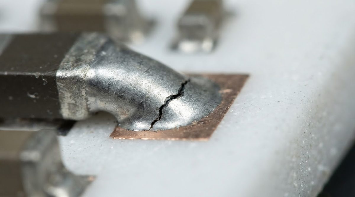
Even on ceramic, poor design shortens thermal cycling life. These practices matter most:
- Minimize unsupported copper area. Large copper planes on DBC boards create high stress at the copper-ceramic edge. Keep copper features at least 0.5 mm from the substrate edge. Dimpled or segmented copper planes reduce peak stress.
- Match component CTE to substrate. Mounting a large LTCC package (CTE ~6 ppm/°C) on alumina (CTE ~7 ppm/°C) yields almost zero mismatch. Mounting a large BGA with organic interposer (CTE ~15 ppm/°C) on ceramic reintroduces the problem.
- Use compliant solder or sintered silver. High-lead or sintered silver die attach absorbs strain better than rigid SAC305 for power die. Sintered silver also survives higher temperatures.
- Control substrate flatness. Warped substrates create uneven solder joints with thin spots that crack first. Warpage and flatness control during fabrication is critical for cycling reliability.
Running thermal simulation on your ceramic board layout before prototyping lets you identify hot spots and strain concentrations that would otherwise appear only after hundreds of test cycles.
When NOT to Use Ceramic for Thermal Cycling
Ceramic is not always the right answer, even when cycling reliability matters.
- Cost-sensitive consumer products with mild thermal profiles. If the operating range is 0 °C to +70 °C and the product life is 5 years with slow ambient changes, FR-4 or MCPCB will likely survive. Ceramic adds cost (3–10× per unit area) that the application does not need.
- Large board areas (>150 mm × 150 mm). Ceramic substrates are brittle and limited in panel size. For large boards, an MCPCB with a high-reliability dielectric or an insulated metal substrate (IMS) may be more practical.
- High-vibration environments without proper mounting. Ceramic’s brittleness means that mechanical shock or vibration can crack the substrate itself, a failure mode FR-4 and MCPCB resist. If vibration is the dominant stress, a flexible or semi-rigid substrate may outperform ceramic despite worse thermal cycling numbers.
- Prototyping speed. FR-4 boards ship in days. Ceramic prototypes take longer. If you need fast iteration and thermal cycling reliability is not yet the gating concern, start on FR-4 and move to ceramic for qualification.
Frequently Asked Questions
How many thermal cycles can a ceramic PCB survive?
96% alumina ceramic PCBs typically survive 3,000–10,000+ cycles at –55/+150 °C before first solder joint or metallization failure, depending on copper thickness, metallization type (DBC vs AMB vs thin film), and solder alloy. AlN substrates often exceed 5,000 cycles under the same profile due to closer CTE match with silicon and GaN die.
Does ceramic PCB delaminate like FR-4?
No. Ceramic substrates are monolithic (single-material) or co-fired, with no organic interlayer that can separate. Delamination is a failure mode specific to laminated substrates like FR-4 and MCPCB dielectric layers. Ceramic failure occurs at the metallization interface or solder joint instead.
Can I use SAC305 solder on ceramic substrates?
Yes. SAC305 is widely used for surface-mount components on ceramic boards. For power die attach where thermal cycling reliability ceramic assemblies demand is critical, sintered silver or high-lead solder (e.g., Pb92.5Sn5Ag2.5) provides longer fatigue life because these materials handle creep strain better than SAC alloys at high temperatures.
What test standard should I use for thermal cycling qualification?
IEC 60068-2-14 Na (temperature change) and JEDEC JESD22-A104 are the most common. Automotive programs often reference AEC-Q200 or customer-specific profiles. Always specify the exact temperature range, ramp rate, dwell time, and pass/fail criteria—cycle-life numbers are meaningless without these details.
Is AlN better than alumina for thermal cycling?
AlN (CTE 4.3–4.6 ppm/°C) matches silicon and GaN more closely than 96% alumina (CTE 6.5–7.2 ppm/°C), so solder joints see less strain per cycle. AlN also conducts heat 6–8× better, lowering junction temperatures and reducing effective ΔT. The trade-off is cost: AlN substrates cost 3–5× more than alumina per unit area.
Next Step
If your application faces more than 1,000 thermal cycles at ΔT > 100 °C, ceramic substrates are worth evaluating. Start by defining your cycling profile and die/component CTEs, then use the comparison tool above to estimate relative cycle life. When you are ready to move forward, browse common ceramic PCB questions or request a quote to discuss your specific reliability requirements.