Ceramic PCB yield ranges from roughly 70% for complex multilayer HTCC/LTCC builds to 95–98% for simple single-layer DPC or thick-film circuits. The gap matters: every point of lost yield adds directly to unit cost, and ceramic substrates already carry a price premium over FR-4. Understanding what drives scrap lets you design for yield and negotiate pricing with data instead of guesswork.
Key Takeaways
- Single-layer alumina DPC boards routinely achieve 93–98% first-pass yield in production volumes.
- Each additional ceramic layer in an LTCC or HTCC stack typically reduces yield by 3–8 percentage points due to cumulative defect probability.
- Substrate cracking during singulation and metallization voids are the two largest scrap categories, together accounting for 40–60% of rejects in most fabs.
- Tightening line/space below 75 µm or requesting AlN instead of Al₂O₃ can cut yield by 10–20% relative to a standard 96% alumina design.
- First article inspection catches systematic defects before they propagate across a lot, often recovering 5–15% of yield that would otherwise be lost.
Typical Yield Ranges by Process and Complexity
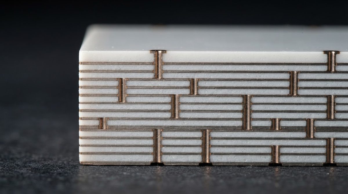
Yield is process-dependent before it is design-dependent. The table below shows ranges observed across commercial ceramic PCB production. These are first-pass yields, meaning boards that pass all electrical and visual inspection without rework.
| Process | Layer count | Typical first-pass yield | Primary scrap mode |
|---|---|---|---|
| DPC (direct plated copper) | 1–2 | 93–98% | Photoresist defects, copper adhesion |
| Thick film (screen print) | 1–2 | 90–96% | Print registration, paste voids |
| Thin film (sputter + etch) | 1–2 | 88–95% | Particle contamination, etch undercut |
| DBC (direct bonded copper) | 1 | 90–96% | Copper delamination, edge voids |
| LTCC | 4–12 | 75–90% | Layer misregistration, delamination |
| HTCC | 4–20+ | 70–88% | Shrinkage mismatch, via fill defects |
Ranges reflect published fab data and industry benchmarks. Actual yield depends on design rules, substrate material, and fab maturity.
The pattern is clear: more layers and finer features compress yield. A 12-layer LTCC RF module with 50 µm vias is a fundamentally different manufacturing challenge than a single-layer alumina power substrate with 200 µm traces. Price should reflect that, and your design choices directly influence where on the curve you land.
The Six Biggest Scrap Drivers
1. Substrate cracking during singulation
Ceramic is brittle. Mechanical scoring, laser scribing, and diamond sawing each impose stress on the substrate edge. Cracks that start at the scribe line can propagate into the circuit area, killing the board. Thinner substrates (below 0.38 mm) and substrates with metallization close to the edge are most vulnerable. Proper laser scribing technique reduces edge chipping by controlling kerf depth and pulse energy, but it cannot eliminate the risk entirely. Design rule: keep copper features at least 0.3 mm from the panel edge or scribe line.
2. Metallization voids and adhesion failures
Whether the metal is screen-printed silver, sputtered TiW/Cu, or directly bonded copper, voids between the metal and the ceramic surface are the second-largest reject category. Causes include surface contamination, insufficient roughening, atmosphere control failures during firing, and moisture absorption in green tape. X-ray inspection of vias and bond interfaces catches subsurface voids that visual inspection misses, but it adds cycle time and cost. For DBC, a typical acceptance criterion is less than 2% void area per die-attach pad, verified by acoustic microscopy or X-ray.
3. Layer-to-layer misregistration (multilayer only)
LTCC and HTCC processes involve stacking and laminating multiple green ceramic sheets, each with its own printed conductor pattern. Registration errors accumulate. A ±25 µm misalignment per layer becomes ±75 µm over three layers, which can short adjacent vias or break a ground plane connection. Multilayer ceramic builds with more than six layers typically require optical alignment systems and tighter incoming tape thickness tolerances to hold registration within spec.
4. Shrinkage variation during co-firing
Green ceramic tape shrinks 12–17% (x-y) and 15–25% (z) during sintering. The exact shrinkage depends on tape composition, particle size distribution, binder burnout profile, and furnace load. Lot-to-lot variation in tape properties can shift shrinkage by 0.3–0.5%, which on a 150 mm panel translates to 0.45–0.75 mm of positional error. This is why lot traceability and serialization matter: if a tape lot drifts, you need to quarantine and disposition only the affected boards, not the entire production run.
5. Substrate material defects
Incoming ceramic substrates can contain pores, inclusions, micro-cracks, or thickness variation outside tolerance. A 96% alumina substrate with a 50 µm pore directly under a high-voltage trace will fail dielectric withstand testing. Incoming inspection with sample-based flexural strength testing (per ASTM C1161) and dimensional checks catches the worst offenders, but some defects only reveal themselves after metallization or thermal processing.
6. Surface finish and solderability defects
ENIG, ENEPIG, and bare gold finishes each have their own failure modes. Black pad syndrome in ENIG, phosphorus segregation in electroless nickel, and gold embrittlement in thick gold plating all reduce yield at the assembly stage rather than the bare-board stage. Solderability testing on ceramic substrates before shipment catches wetting failures early, preventing expensive rework downstream.
Worked Example: How Yield Affects Unit Cost
Suppose you order 1,000 pieces of a single-layer DPC board on 96% alumina. The panel holds 12 boards. Raw material, processing, and inspection cost $18.00 per panel.
At 95% yield, you get 11.4 good boards per panel on average. You need 88 panels to deliver 1,000 good boards. Total cost: 88 × $18 = $1,584, or $1.58 per board.
At 85% yield (say you tightened line/space to 50 µm), you get 10.2 good boards per panel. You need 98 panels. Total cost: 98 × $18 = $1,764, or $1.76 per board. That 10-point yield drop raised unit cost by 11%.
Now imagine a 6-layer LTCC at 80% yield with a panel cost of $95. You get 9.6 good per panel, need 105 panels for 1,000 boards: $9,975 total, $9.98 per board. Drop yield to 72% (add two more layers or tighter vias) and the same order costs $11,020, or $11.02 per board. Every yield point is worth roughly $0.13 per board in this scenario.
How to Improve Ceramic PCB Yield
Design for the process, not the limit. If your fab quotes 75 µm minimum trace/space, design at 100 µm where the layout allows. The yield difference between “can do” and “comfortable” is substantial.
Panelize intelligently. Larger panels amortize setup cost but increase the chance that a single defect kills multiple boards. Smaller panel arrays with well-placed scribe lines and adequate edge clearance often deliver better net yield.
Specify incoming substrate inspection. Require the substrate vendor to supply C-scan or transmission data for AlN substrates, and flexural strength coupons per lot for alumina. This catches material-driven scrap before you add value.
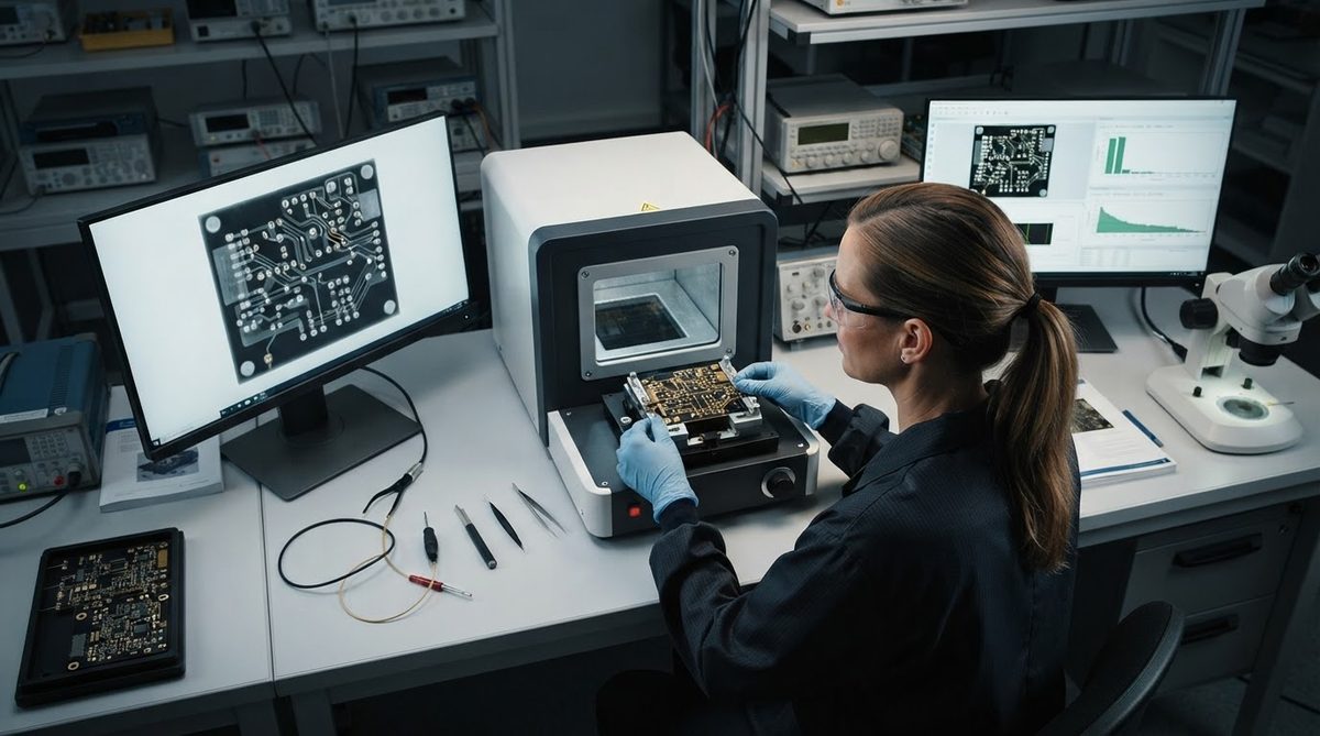
Run a proper FAI. A ceramic PCB first article inspection on the initial panels identifies registration drift, shrinkage offset, and metallization issues before the full lot runs. Correcting a furnace profile after 5 panels is cheap; scrapping 200 panels is not.
Control the singulation step. If your design allows it, prefer laser scribing over mechanical breaking for substrates thinner than 0.5 mm. For thicker substrates, diamond wheel dicing with coolant gives cleaner edges than snap-breaking along score lines.
When Yield Concerns Should Push You Away from Ceramic
If your design requires more than 12 layers with sub-50 µm features, expect yield below 75% and high unit cost. At that complexity level, consider whether an LTCC substrate is truly necessary or whether a hybrid approach (ceramic interposer plus organic redistribution layer) gives equivalent performance at higher yield. For RF front-end modules below 6 GHz, high-frequency laminates like Rogers RO4000 series may meet your loss tangent requirements at far higher manufacturing yield. And if your volume exceeds 50,000 units per year with modest thermal or frequency demands, FR-4 or metal-core PCB will almost always win on cost per board, even after accounting for the performance gap.
FAQ
What is a normal scrap rate for ceramic PCBs?
A scrap rate of 2–10% is typical for single- and double-layer ceramic boards in mature production. Multilayer LTCC and HTCC builds commonly see 10–30% scrap, depending on layer count and feature size. These figures assume a qualified process with stable incoming material.
Does AlN have worse yield than alumina?
Yes, generally. Aluminum nitride is harder to metallize, more sensitive to moisture, and more expensive per substrate, so defects cost more and occur more often. Expect 3–8 percentage points lower yield compared to 96% alumina for the same circuit design and process.
Can rework recover scrapped ceramic boards?
Sometimes, but only for specific defect types. A metallization defect on a thick-film board can occasionally be re-fired or re-printed. A cracked substrate is always scrap. Thin-film and DPC boards are rarely reworkable because stripping and re-depositing metal risks damaging the ceramic surface.
How does via fill quality affect yield?
Incomplete via fills are a leading cause of open circuits in multilayer ceramic PCBs. Voids inside a via increase resistance and can crack under thermal cycling. Via fill is typically inspected by X-ray, with acceptance criteria of less than 5–10% void area depending on the application standard (e.g., MIL-PRF-55681 for military LTCC).
Should I ask my supplier for yield data?
Yes. Request first-pass yield and final yield (after any rework) for your specific part number, not a factory average. A supplier who tracks and shares lot-level yield data is more likely to maintain process control. Yield trending over multiple lots is more informative than a single number.
Next Step
If you are estimating cost for a ceramic PCB project, yield is one of the largest variables. Share your Gerber files and specifications for a quote that reflects realistic yield assumptions for your specific design, rather than generic factory averages.