Aluminum nitride AlN CTE sits at 4.4–5.2 ppm/°C over the 25–400 °C range, per ASTM E228 dilatometry. That value is close to silicon (2.6 ppm/°C), gallium nitride (3.2 ppm/°C), and silicon carbide (4.0 ppm/°C), which is why AlN is the default ceramic substrate for high-power die attach where CTE mismatch drives solder-joint fatigue. Understanding aluminum nitride AlN CTE behavior across temperature and purity grades is essential for reliable power-module design.
Key Takeaways
- Aluminum nitride AlN CTE is 4.4–5.2 ppm/°C (25–400 °C), roughly half that of 96% alumina (6.5–7.0 ppm/°C) and one-third that of copper (16.5 ppm/°C).
- The CTE gap between AlN and a bare silicon die is only ~1.8–2.6 ppm/°C, small enough to survive thousands of thermal cycles in AuSn or sintered-silver attach.
- CTE mismatch stress is proportional to ΔT × ΔCTE × die size. A 5 mm × 5 mm GaN HEMT on AlN sees roughly 60% less thermomechanical stress than the same die on alumina.
- AlN’s CTE advantage matters most above 150 °C junction temperature and for die larger than 3 mm on a side.
What Is CTE and Why Does It Matter for Substrates?
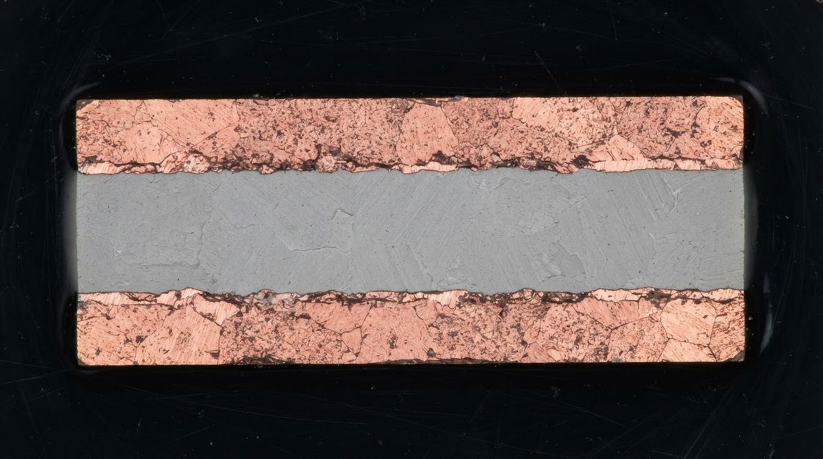
CTE (coefficient of thermal expansion) describes how much a material grows per degree of temperature change, expressed in ppm/°C. When a semiconductor die is soldered to a substrate, both expand during operation. If their CTEs differ significantly, shear stress builds in the solder layer with every power cycle. Over hundreds or thousands of cycles, that stress nucleates cracks, increases thermal resistance, and eventually causes open-circuit failure.
The magnitude of this stress depends on three variables: the CTE difference (ΔCTE), the temperature swing (ΔT), and the lateral dimension of the bonded area. Larger die on mismatched substrates fail faster. This is why power-module designers care intensely about substrate CTE, and why AlN material properties make it a preferred choice for die attach.
Aluminum Nitride AlN CTE Compared to Common Die and Substrate Materials
| Material | CTE (ppm/°C) | Temp. Range | Source |
|---|---|---|---|
| Silicon (Si) | 2.6 | 25–300 °C | NIST SRD |
| Gallium Nitride (GaN) | 3.2 (a-axis) | 25–400 °C | Wolfspeed app note |
| Silicon Carbide (SiC) | 4.0 | 25–400 °C | Wolfspeed / Cree |
| Aluminum Nitride (AlN) | 4.4–5.2 | 25–400 °C | Kyocera / Maruwa datasheets |
| Alumina 96% (Al₂O₃) | 6.5–7.0 | 25–400 °C | CoorsTek datasheet |
| Silicon Nitride (Si₃N₄) | 2.5–3.4 | 25–400 °C | Kyocera SN series |
| Copper (Cu) | 16.5 | 20 °C | ASM Handbook |
| Gold-Tin solder (AuSn) | 16.0 | 20 °C | Indium Corp. datasheet |
Typical values for commercially available material, for comparison only. Confirm against the datasheet for your specific grade.
The aluminum nitride AlN CTE sweet spot is clear in this table: close enough to Si, GaN, and SiC to keep mismatch stress low, yet far enough from copper that the metallization layer (typically thin-film Ti/Pt/Au or DPC Cu) acts as a compliant buffer rather than a stress driver. For a deeper look at how different AlN purity grades affect CTE and thermal conductivity, see our grades comparison.
Worked Example: CTE Mismatch Stress in a Die-Attach Joint
A simplified elastic model (Timoshenko bimetallic strip, adapted for die attach) estimates the peak shear stress at the edge of a bonded die:
τ_max ≈ (ΔCTE × ΔT × G_solder × L) / (2 × t_solder)
Where L is the half-length of the die, t_solder is solder thickness, and G_solder is the shear modulus of the solder.
Case: 5 mm × 5 mm SiC die, ΔT = 200 °C, AuSn solder (G ≈ 25 GPa), solder thickness = 25 µm.
- On AlN (ΔCTE = 1.0 ppm/°C): τ_max ≈ (1.0 × 10⁻⁶ × 200 × 25 × 10⁹ × 2.5 × 10⁻³) / (2 × 25 × 10⁻⁶) = 250 MPa
- On Al₂O₃ 96% (ΔCTE = 3.0 ppm/°C): τ_max ≈ 750 MPa
The alumina case exceeds the shear strength of AuSn (~275 MPa), meaning cracking is likely within the first few hundred cycles. The AlN case stays within the elastic limit. This is a simplified model; finite-element analysis with creep behavior gives more accurate cycle-life predictions, but the directional conclusion holds: 3× lower ΔCTE translates to roughly 3× lower peak shear stress and an order-of-magnitude improvement in fatigue life.
Enter your substrate material, die size, solder type, and temperature swing below to estimate the peak shear stress and compare AlN against alumina for your specific design.
How Aluminum Nitride AlN CTE Varies with Temperature and Grade
AlN’s CTE is not constant. It rises with temperature. At room temperature, CTE is approximately 4.4 ppm/°C. By 400 °C it reaches about 5.2 ppm/°C. By 800 °C, some grades report 5.6–5.8 ppm/°C per Maruwa’s high-purity AlN datasheet. This means the effective CTE over a thermal cycle depends on the actual temperature swing your device sees.
Purity also matters. Lower-purity AlN (below 95%) contains yttria or other sintering aids that form grain-boundary phases with slightly higher CTE. High-purity AlN (≥99%) has a tighter CTE range and better thermal conductivity (170–200 W/mK vs. 140–170 W/mK). For the full property comparison, see the AlN substrate datasheet.
CTE Matching Strategies for AlN Substrates
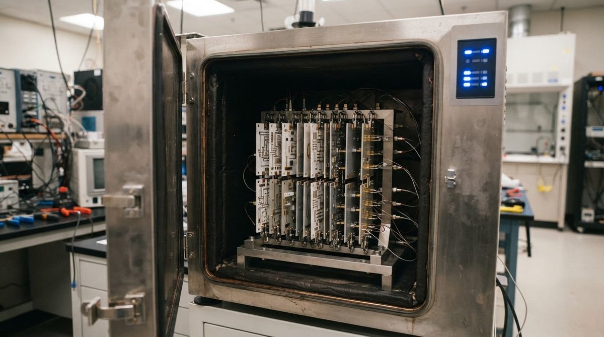
Choose the Right Attach Material
AuSn (80/20) is rigid and transmits CTE mismatch stress directly. It works well with AlN because the aluminum nitride AlN CTE gap to common die materials is small. For larger die (>10 mm) or extreme cycling, sintered silver or active metal brazing provides a more compliant joint. SAC305 solder has a lower modulus but introduces creep and lower melting point, limiting its use above 150 °C.
Control Substrate Thickness
A thinner AlN substrate is more compliant and absorbs less strain energy. For die attach, 0.25 mm and 0.38 mm substrates are common. A 0.635 mm substrate is stiffer and may be preferable for mechanical support, but increases the CTE-driven bending moment. Consult our guide on AlN substrate thickness options for available dimensions and tolerances.
Manage Copper Layer CTE
In DBC (direct bond copper) or AMB (active metal brazing) constructions, the copper layer has a CTE of 16.5 ppm/°C. The effective CTE of the copper-AlN-copper sandwich depends on copper thickness. Thicker copper shifts the composite CTE upward, which can actually help match to a copper baseplate but hurts die-side matching. Balanced copper on both sides minimizes warpage. For broader guidance on CTE matching across ceramic substrates, see CTE matching in ceramic PCB design.
When NOT to Use AlN for CTE Matching
AlN is not always the right substrate. Consider alternatives in these cases:
- Die smaller than 2 mm on a side with ΔT below 100 °C: CTE mismatch stress is low enough that 96% alumina works fine at a fraction of the cost.
- Extreme mechanical shock or vibration: AlN has a flexural strength of 300–400 MPa, adequate for most electronics but lower than silicon nitride (Si₃N₄) substrates at 600–900 MPa. If fracture toughness is the primary concern, Si₃N₄ is a better choice despite its higher cost.
- Budget-constrained, high-volume consumer products: AlN substrates cost 3–5× more than alumina per unit area. If thermal performance is adequate on alumina or metal-core PCB, the CTE benefit of AlN does not justify the premium.
- Very low-frequency, low-power RF: If your design does not generate significant thermal cycling, CTE matching is irrelevant and FR-4 or standard MCPCB is sufficient.
Frequently Asked Questions
Does AlN CTE match silicon exactly?
No. Aluminum nitride AlN CTE is 4.4–5.2 ppm/°C while silicon is 2.6 ppm/°C, a gap of about 1.8–2.6 ppm/°C. This is close enough for reliable die attach with AuSn or sintered silver across thousands of thermal cycles, but it is not a perfect match. Si₃N₄ (2.5–3.4 ppm/°C) is closer to silicon if that gap is critical.
Can I use SAC305 solder to attach a die to AlN?
Yes, but with limits. SAC305 melts at 217–220 °C, restricting operation to about 150 °C junction temperature. Its lower shear modulus reduces CTE mismatch stress compared to AuSn, but it creeps under sustained load. For high-reliability applications above 150 °C, AuSn or sintered silver is preferred.
How does AlN CTE compare to BeO?
Beryllium oxide has a CTE of about 6.7–7.4 ppm/°C, similar to alumina and significantly higher than AlN. AlN is the better CTE match to Si, GaN, and SiC die. BeO’s advantage is its high thermal conductivity (250–300 W/mK), but beryllium oxide dust is a confirmed human carcinogen and causes chronic beryllium disease. Its use is heavily restricted and requires special handling.
Does copper metallization change the effective CTE of an AlN substrate?
Yes. A DBC or AMB copper layer shifts the composite CTE upward. For example, a 0.3 mm Cu / 0.635 mm AlN / 0.3 mm Cu stack has an effective in-plane CTE of roughly 7–9 ppm/°C, depending on temperature. This is significantly higher than bare AlN and must be accounted for in die-attach stress analysis.
What test standard measures CTE for ceramic substrates?
ASTM E228 (push-rod dilatometry) is the most common method. Some manufacturers also use ASTM E831 (TMA). Always check which standard and temperature range the reported CTE value refers to, since CTE varies with temperature.
Next Step
If you are designing a power module or high-reliability assembly and need AlN substrates with controlled CTE matching, request a quote with your die size, operating temperature range, and metallization requirements. We can recommend the right AlN grade and thickness for your thermal cycle profile.