Alumina 99.6% Al2O3 laser scribed substrates are the standard approach for pre-scoring high-purity ceramic panels so they snap apart cleanly after metallisation and component attach. A CO₂ or Nd:YAG laser ablates a V-groove—typically 40–80 µm wide and 30–50% of substrate thickness deep—along programmed lines. The substrate then breaks along those grooves with positional accuracy of ±25 µm or better, producing smooth edges with minimal micro-cracking.
Key Takeaways
- Alumina 99.6% Al2O3 laser scribed grooves achieve positional accuracy of ±25 µm, tighter than mechanical scribing (±50–75 µm).
- Scribe depth is typically 30–50% of substrate thickness; going deeper risks spontaneous fracture during handling.
- 99.6% Al2O3 scribes more cleanly than 96% alumina because its finer grain structure (1–3 µm vs. 5–15 µm) produces fewer edge chips.
- Minimum recommended keep-out from a scribe line to the nearest conductor is 200 µm for thin-film circuits and 300 µm for thick-film.
- Laser scribing is a non-contact process—no mechanical stress is applied to the substrate until the final snap step.
Why Choose Alumina 99.6% Al2O3 Laser Scribed Panels?
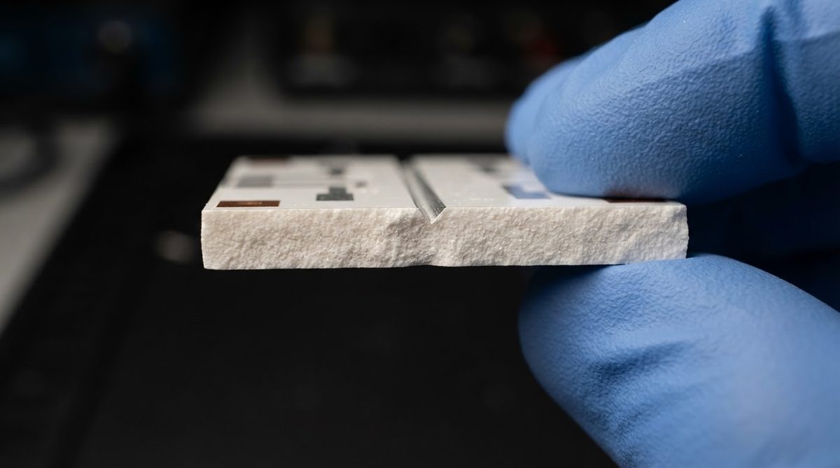
High-purity alumina (99.6% Al2O3) has a dense, fine-grained microstructure. Average grain size sits between 1 and 3 µm, compared with 5–15 µm for standard 96% alumina (per CoorsTek ADS-996 datasheet). Smaller grains mean the fracture path during snap separation follows a more predictable line, reducing edge chipping to under 25 µm in most cases.
The higher purity also matters electrically. With a dielectric constant of 9.7–9.9 at 1 MHz and loss tangent below 0.0002, 99.6% alumina is preferred for RF hybrid circuits and precision sensor substrates where even minor compositional variation can shift impedance. Laser scribing preserves these properties because it introduces no binder, coolant, or mechanical contamination.
If your application needs the thermal performance of alumina but demands a surface finish before scribing, polished and lapped 99.6% alumina substrates can be laser-scribed after polishing with no degradation of Ra values away from the groove.
Laser Scribing Process Step by Step
- Panel inspection. Incoming 99.6% Al2O3 panels (typically 100 × 100 mm to 150 × 150 mm) are checked for warpage (<0.1 mm per 25 mm) and surface defects.
- Laser setup. A CO₂ laser (wavelength 10.6 µm) or Nd:YAG laser (1.064 µm) is focused to a spot size of 30–60 µm. Power, pulse rate, and traverse speed are set to achieve the target groove depth.
- Scribing. The laser traces programmed X-Y paths. Multiple passes may be used for thicker substrates (≥0.635 mm) to control heat input and avoid micro-crack propagation beyond the groove.
- Cleaning. Ablation debris (recast alumina) is removed by ultrasonic cleaning in DI water or gentle air-knife, preventing contamination of subsequent metallisation.
- Metallisation and assembly. Thin-film (sputtered) or thick-film (screen-printed) conductors are applied to the scribed panel.
- Snap separation. A three-point break fixture applies controlled bending force. The substrate fractures along the scribe line.
Scribe Groove Specifications for Alumina 99.6% Al2O3 Laser Scribed Substrates
| Parameter | Typical Value | Unit | Condition | Source |
|---|---|---|---|---|
| Groove width | 40–80 | µm | CO₂ laser, single pass | Kyocera A-493 datasheet |
| Groove depth | 30–50% of thickness | — | 0.25–1.0 mm substrates | Industry standard practice |
| Positional accuracy | ±25 | µm | Galvo-steered laser | CoorsTek ADS-996 application note |
| Edge chip size after snap | <25 | µm | 99.6% Al2O3, 0.635 mm thick | Maruwa HA-996 datasheet |
| Minimum scribe pitch | 2.0 | mm | Substrate ≥0.25 mm thick | General industry guideline |
| Surface roughness of groove wall | 1.0–2.5 | µm Ra | As-scribed, no post-process | Measured, typical |
Typical values for commercially available material, for comparison only. Confirm against the datasheet for your specific grade.
Enter your substrate thickness and desired scribe depth percentage to see the recommended laser parameters and expected edge chip size for alumina 99.6% Al2O3 laser scribed panels.
Design Rules for Alumina 99.6% Al2O3 Laser Scribed Panels
Keep-out zone. Maintain at least 200 µm clearance between any scribe line and the nearest thin-film trace. For thick-film conductors, increase this to 300 µm. The snap fracture can deviate by up to ±25 µm, and any conductor crossing the fracture zone will crack or delaminate.
Via and hole placement. Laser-drilled or punched vias should be no closer than 500 µm to a scribe line. Vias nearer than this concentrate stress and can cause the substrate to crack prematurely during handling.
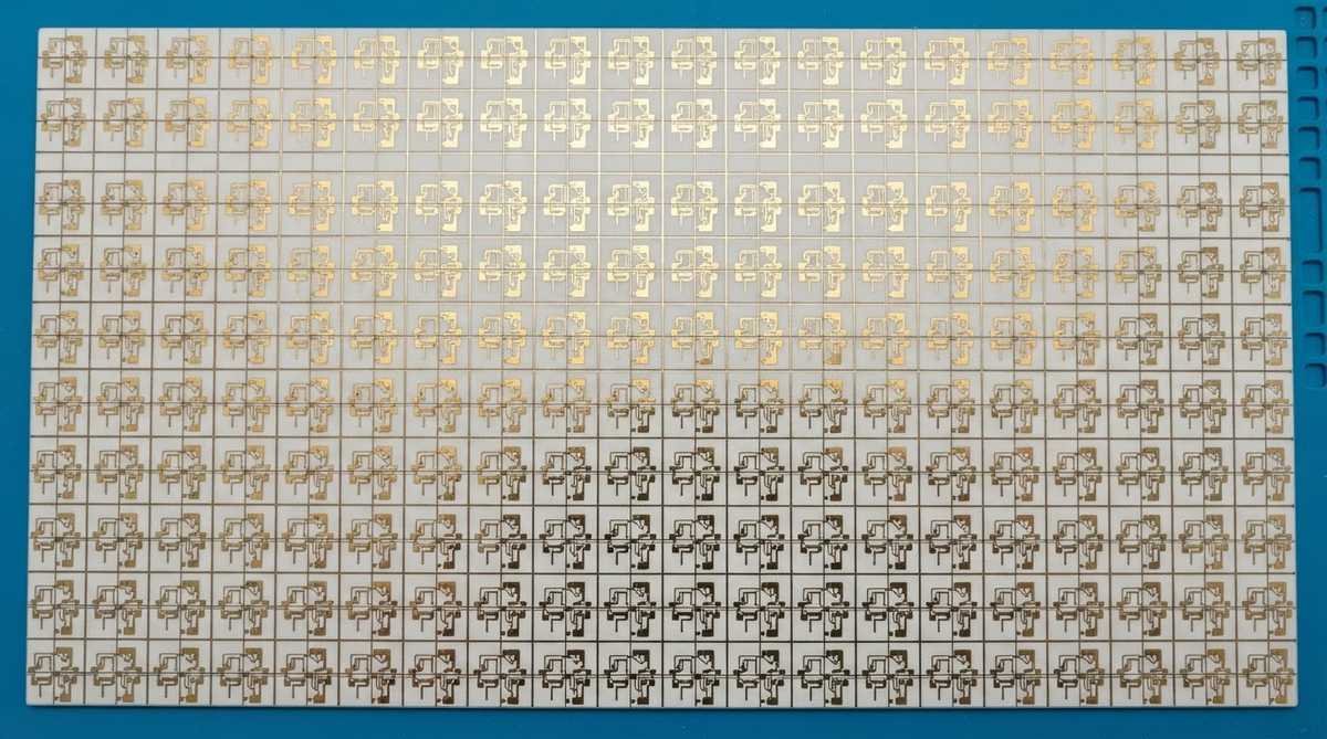
Panel utilisation. Scribe streets consume 0.1–0.15 mm of width (the groove itself) plus the keep-out on each side. For a 5 × 5 mm unit on a 100 × 100 mm panel with 0.2 mm keep-out per side, you lose roughly 0.5 mm per street. Plan your array to maximise yield; a 0.5 mm reduction in street width across 20 streets saves 10 mm of panel real estate.
Laser Scribing vs. Mechanical Scribing on 99.6% Al2O3
| Parameter | Laser Scribing | Mechanical (Diamond) Scribing |
|---|---|---|
| Positional accuracy | ±25 µm | ±50–75 µm |
| Edge chip size | <25 µm | 25–75 µm |
| Minimum groove pitch | 2.0 mm | 3.0 mm |
| Contact with substrate | Non-contact | Contact (blade wear) |
| Tooling cost | Higher capital, no consumable blade | Lower capital, blade replacement |
| Throughput (panels/hr) | 60–120 (depends on pattern) | 100–200 |
| Best suited for | Fine-pitch, thin-film, RF hybrids | Large panels, simple grid patterns |
For most thin-film and RF hybrid applications on 99.6% alumina, laser scribing is the better choice. The tighter edge quality and positional accuracy justify the higher capital cost. Mechanical scribing still makes sense for high-volume, simple grid singulation where edge quality is less critical.
Comparing Laser-Scribed Substrates Across Ceramic Materials
If alumina 99.6% Al2O3 laser scribed substrates do not meet your thermal or mechanical requirements, other ceramics can also be laser scribed. Aluminum nitride (AlN) laser-scribed substrates offer 170–200 W/mK thermal conductivity versus 28–35 W/mK for 99.6% alumina, but at three to five times the cost. Silicon nitride (Si₃N₄) laser-scribed substrates provide far higher fracture toughness (6–7 MPa·√m vs. 3.5–4.0 MPa·√m for alumina) and are the go-to for power modules subjected to thermal cycling. Use our ceramic substrate selection guide to compare all options side by side.
When Not to Use Laser-Scribed 99.6% Alumina
Very thick substrates (>1.5 mm). Laser groove depth is limited. At these thicknesses, diamond saw dicing is more reliable than scribe-and-snap.
Curved or non-linear separation paths. Laser scribing produces straight lines only. If you need curved outlines, laser cutting (full-through) or waterjet is required.
Cost-sensitive, non-critical applications. Standard 96% alumina costs 30–40% less per panel. If you do not need the finer grain structure, higher purity, or tighter dielectric tolerance, 96% alumina with laser scribing will perform adequately.
Extreme thermal loads. If your heat flux exceeds what 28–35 W/mK can handle, switch to AlN or consider a DBC (direct bond copper) on AlN architecture.
FAQ
Can I laser-scribe a substrate that already has metallisation on it?
Yes, but it is not recommended. Scribing after metallisation risks metal splash, recast debris on conductors, and micro-cracking under traces. Standard practice is to scribe the bare substrate first, then metallise the panel, then snap-separate.
What is the thinnest 99.6% alumina substrate that can be laser scribed?
Substrates as thin as 0.25 mm (250 µm) are routinely laser scribed. Below 0.25 mm, handling fragility becomes the limiting factor rather than the scribing process itself.
Does laser scribing affect the dielectric properties of the substrate?
No measurable change occurs outside the groove zone. The heat-affected zone extends only 10–20 µm from the groove wall. Bulk dielectric constant and loss tangent remain within datasheet specification.
How do I specify scribe lines on my drawing?
Provide scribe line positions as X-Y coordinates referenced to a datum corner, with a tolerance callout (e.g., ±25 µm). Indicate scribe depth as a percentage of substrate thickness. Include keep-out zones as hatched areas on the metallisation layer.
Is laser scribing available on panels larger than 150 × 150 mm?
Some equipment handles panels up to 200 × 200 mm, but availability depends on the manufacturer’s stage size. For larger panels, confirm with your supplier before committing your panel layout.