Ceramic PCBs operate reliably at cryogenic temperatures—down to 4 K (−269 °C) in some cases—because the substrate itself does not soften, outgas, or delaminate the way organic laminates do. Alumina (Al₂O₃), aluminum nitride (AlN), and silicon nitride (Si₃N₄) all retain structural integrity well below −196 °C (liquid nitrogen), making ceramic the default substrate family for superconducting electronics, space-borne infrared sensors, and quantum computing modules.
Key Takeaways
- 96 % alumina remains mechanically stable to at least 4 K, with a CTE that drops from ~6.5 ppm/°C at 25 °C to effectively zero below 30 K (per CoorsTek ADS-96R datasheet).
- AlN thermal conductivity increases as temperature falls, peaking above 1 000 W/m·K near 40–80 K in high-purity single-crystal samples (Slack, 1973), though polycrystalline substrates peak at roughly 300–600 W/m·K.
- CTE mismatch between ceramic and metallization is the primary failure mode at cryogenic temperatures, not the ceramic itself.
- FR-4 glass transition starts near 130–170 °C but embrittlement below −40 °C makes it unsuitable for true cryogenic service; polyimide flex survives somewhat lower but still outgasses under vacuum.
- Solder joints, wire bonds, and adhesive die-attach layers fail before the ceramic substrate does.
Why Organic Laminates Fail at Cryogenic Temperatures
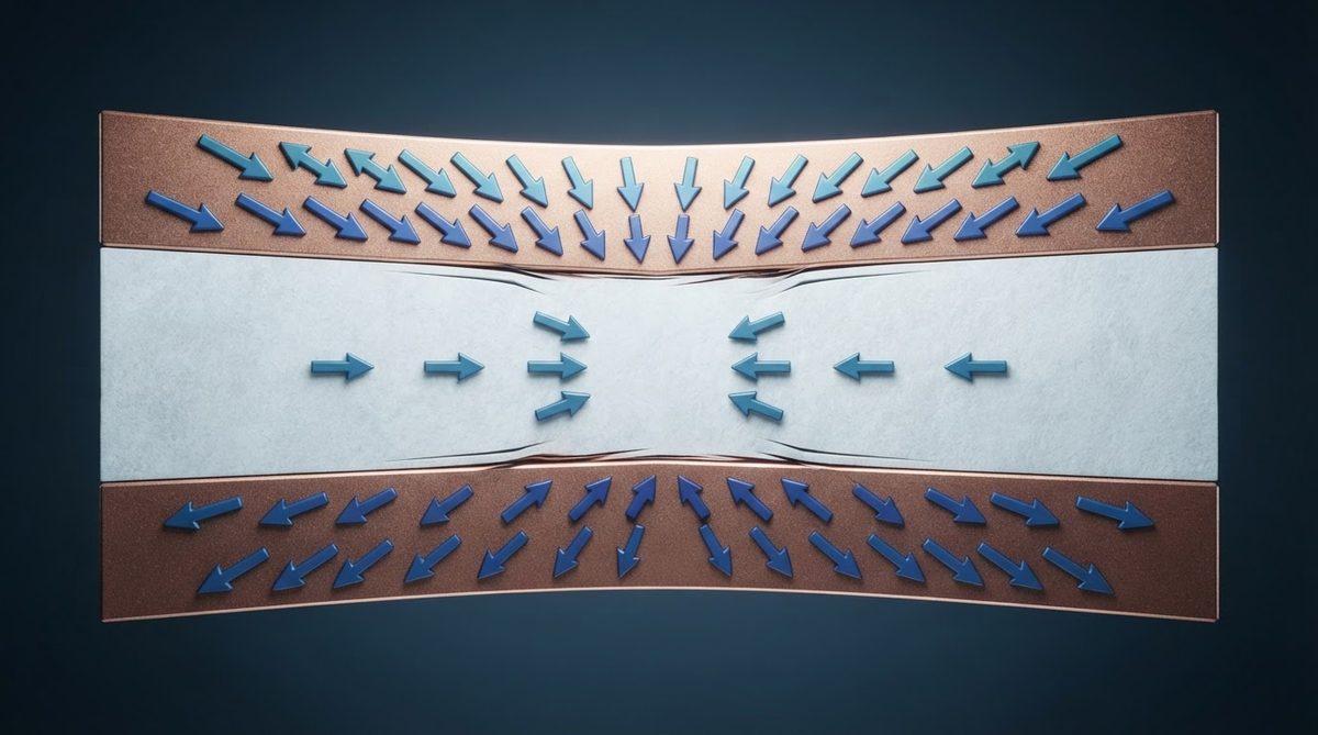
FR-4 and polyimide laminates rely on epoxy or polyimide resin to bind glass-fiber reinforcement. Below roughly −60 °C the resin becomes glassy and brittle. Plated-through holes crack because the Z-axis CTE of FR-4 (~60 ppm/°C above Tg) freezes unevenly, locking in residual stress. At liquid-nitrogen temperatures (−196 °C), microcracking in the resin is almost guaranteed, and outgassing in vacuum environments contaminates nearby optics or detectors.
Ceramic substrates avoid every one of these mechanisms. There is no resin, no glass transition, and negligible outgassing. The substrate is a monolithic oxide or nitride that was sintered above 1 500 °C. Cooling it to 4 K does not introduce any new phase or structural change.
How Ceramic Properties Change Below −150 °C
Properties do not stay constant across a 300-degree swing. Engineers need the actual curves, not room-temperature numbers.
CTE Contraction
The coefficient of thermal expansion of all ceramics falls toward zero as temperature approaches absolute zero, following the Debye model. For 96 % alumina, CTE at 25 °C is roughly 6.5 ppm/°C. At 77 K (−196 °C) it drops to approximately 1.5–2.0 ppm/°C. Below 30 K it is effectively zero. This means the total integrated contraction from 300 K to 4 K is only about 0.07–0.09 % linear, roughly half the contraction of copper over the same range (~0.33 %). That mismatch is where solder-joint and metallization stress originates.
Thermal Conductivity
Thermal conductivity of crystalline ceramics rises as temperature drops—phonon mean free path increases when fewer phonons are available to scatter. AlN shows the most dramatic effect. Polycrystalline AlN substrates (170–200 W/m·K at 25 °C) can reach 300–600 W/m·K near 50–80 K depending on grain size and oxygen content, per data published by Slack and others (G. A. Slack, Journal of Physics and Chemistry of Solids, 1973). Alumina sees a more modest rise, from ~24–28 W/m·K at 25 °C to roughly 40–80 W/m·K near 50 K. Si₃N₄ thermal conductivity at room temperature (60–90 W/m·K for high-purity grades) also increases at cryogenic temperatures, though published cryogenic data for commercial Si₃N₄ substrates is sparse.
Dielectric Properties
Dielectric constant (εr) of alumina decreases slightly at cryogenic temperatures—from ~9.8 at 25 °C and 1 MHz to roughly 9.4–9.6 at 77 K—because lattice polarizability decreases. Loss tangent also drops, which is favorable for RF and microwave circuits. This is one reason ceramic substrates are preferred in cryogenic low-noise amplifiers for radio astronomy.
| Parameter | Al₂O₃ 96 % (25 °C) | Al₂O₃ 96 % (77 K) | AlN (25 °C) | AlN (77 K) | Unit | Source |
|---|---|---|---|---|---|---|
| Thermal conductivity | 24–28 | 40–80 | 170–200 | 300–600 | W/m·K | CoorsTek ADS-96R; Slack 1973 |
| CTE | 6.5 | 1.5–2.0 | 4.5 | ~1.0 | ppm/°C | CoorsTek; Kyocera SH-30 |
| Flexural strength | 340–380 | ≥ 380 (typically rises) | 300–350 | ≥ 350 | MPa | CeramTec Rubalit; Kyocera |
| Dielectric constant (1 MHz) | 9.8 | ~9.5 | 8.8 | ~8.5 | — | Maruwa; published literature |
Typical values for commercially available material, for comparison only. Confirm against the datasheet for your specific grade.
CTE Mismatch: The Real Failure Mode
The ceramic substrate will not crack from cold alone. What fails is the interface between materials with different contraction rates. Copper metallization contracts roughly 0.33 % from 300 K to 4 K. Alumina contracts about 0.08 %. That ~0.25 % differential over a 10 mm trace length equals 25 µm of shear displacement at the bond line.
For DBC (direct bond copper) substrates, the copper-to-ceramic bond is strong enough to survive many thermal cycles between room temperature and 77 K, but repeated cycling to 4 K can nucleate fatigue cracks at the copper-ceramic interface. Thin-film metallization (sputtered Ti/Pt/Au or Cr/Au) handles cryogenic cycling better because the metal layer is thin enough (typically < 5 µm total) that the absolute contraction difference is negligible. This is why superconducting electronics almost always use thin-film processes on alumina or AlN.
Solder joints are another weak link. SnPb eutectic solder becomes brittle below about −40 °C. SAC305 (lead-free) is even worse—its ductility drops sharply below −20 °C. For cryogenic assemblies, indium solder (melting point 157 °C, ductile to below 4 K) or gold-tin (Au80Sn20) eutectic is standard. Selecting the right solder is at least as important as selecting the right substrate. For an overview of how ceramic substrates handle temperature extremes, including the high end, see our reference page.
Worked Example: Thermal Stress on a 25 mm Alumina Substrate Cooled to 77 K
Assume a 25 × 25 mm, 0.635 mm thick 96 % alumina substrate with 0.3 mm DBC copper, cooled from 300 K to 77 K (ΔT = 223 K).
- Integrated linear strain, copper: ε_Cu ≈ 16.5 ppm/°C × 223 K ≈ 0.368 % (using average CTE over the range, per NIST cryogenic data).
- Integrated linear strain, alumina: ε_Al₂O₃ ≈ 4.0 ppm/°C (average) × 223 K ≈ 0.089 %.
- Differential strain: Δε ≈ 0.279 %, or 2 790 ppm.
- Over 25 mm, this is ~70 µm of differential contraction. The copper wants to shrink 70 µm more than the ceramic does.
- Resulting biaxial stress in the copper (constrained): σ ≈ E_Cu × Δε ≈ 120 GPa × 0.00279 ≈ 335 MPa—above the yield strength of annealed copper (~70 MPa), so the copper will yield plastically on every cool-down.
This is why cryogenic DBC substrates are often limited to thin copper (≤ 127 µm) or use thin-film metallization instead. If your design requires thick copper for high current at cryogenic temperatures, consider high thermal conductivity substrates like AlN with AMB (active metal brazing), which uses a compliant braze layer that absorbs more strain.
Design Rules for Cryogenic Ceramic PCBs
- Metallization: Prefer thin-film (sputtered or evaporated) for cycling below −100 °C. If thick copper is required, keep it under 127 µm and use stress-relief patterns (slotted planes, curved traces).
- Solder: Use indium or AuSn for joints that must survive below −40 °C. Avoid SAC305.
- Wire bonds: Gold ball bonds on gold pads remain reliable to 4 K. Aluminum wedge bonds also work but are more sensitive to contamination.
- Substrate material: AlN is preferred where heat must be extracted at cryogenic temperatures (e.g., cooling a cryogenic HEMT). Alumina is adequate and cheaper when thermal conductivity is less critical.
- Via design: Filled vias with matched-CTE fill material reduce the risk of via cracking. See guidance on thermal via design for fill strategies.
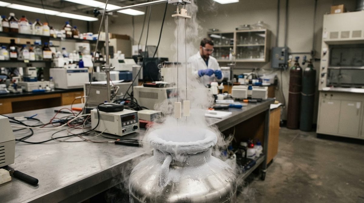
- Thermal cycling qualification: Per MIL-STD-883 Method 1010, Condition C (−65 °C to +150 °C, 100 cycles minimum). For deeper cryogenic service, custom profiles to 77 K or 4 K with at least 500 cycles are common in space and quantum programs.
When NOT to Use Ceramic at Cryogenic Temperatures
Ceramic is the right call for most cryogenic electronics, but there are exceptions.
- Large-area boards (> 100 × 100 mm): Ceramic substrates are typically limited to ~150 × 150 mm maximum. If your cryogenic system needs a large motherboard, you may need a tiled ceramic approach or a cryogenic-rated polyimide flex (Kapton survives to 4 K in some configurations, though with higher dielectric loss).
- High-density digital logic: If you need 1 000+ vias and fine-pitch BGA, FR-4 alternatives like Rogers RO4000 series (rated to −40 °C) or specialized cryogenic laminates may be more practical, provided you stay above −55 °C.
- Cost-sensitive prototypes above −55 °C: Standard polyimide PCBs handle −55 °C adequately per IPC-6012 Class 3. Ceramic is overkill if you never go below that.
Running a Thermal Model for Cryogenic Conditions
Standard thermal simulation tools (ANSYS, COMSOL) support temperature-dependent material properties, but you must supply the cryogenic curves yourself—default material libraries typically stop at −40 °C or 0 °C. NIST publishes cryogenic thermal conductivity and CTE data for copper, alumina, and AlN in their Cryogenic Material Properties database. Feed those curves into your model. For guidance on setting up a ceramic board thermal model, see our article on thermal simulation for ceramic PCBs.
FAQ
Can I reflow-solder components onto a ceramic PCB that will operate at 4 K?
Yes, but use indium-based solder (In or InSn) rather than SAC305 or SnPb. Indium remains ductile to below 1 K. Standard lead-free solders become brittle below −20 °C and will crack under thermal cycling to 4 K.
Does alumina become more brittle at cryogenic temperatures?
Alumina flexural strength actually increases slightly at cryogenic temperatures—ceramic does not undergo a ductile-to-brittle transition because it is already brittle at room temperature. The risk is not the ceramic cracking from cold; it is stress from CTE-mismatched layers bonded to it.
Is AlN always better than alumina for cryogenic PCBs?
AlN is better when you need to extract heat at cryogenic temperatures, because its thermal conductivity rises dramatically below 100 K. If the board is purely a signal carrier with negligible power dissipation, 96 % alumina works fine and costs three to five times less per substrate.
What about LTCC for cryogenic applications?
LTCC (low-temperature co-fired ceramic) has been used successfully in cryogenic microwave circuits, including at 4 K. The glass-ceramic composition of LTCC does not undergo phase changes at low temperatures. However, the embedded silver or gold conductors still create CTE mismatch stress, so layer count and conductor thickness must be managed carefully.
How many thermal cycles can a ceramic PCB survive between 300 K and 4 K?
The ceramic itself can survive indefinitely. The metallization and solder joints are the limiting factor. Thin-film metallized alumina substrates have been qualified to over 10 000 cycles between 300 K and 77 K in published studies for space cryocooler electronics. DBC substrates with thick copper typically survive 500–2 000 cycles to 77 K before interface fatigue becomes measurable.
Do I need hermetic packaging for a cryogenic ceramic PCB?
In vacuum cryostats, hermetic packaging of the PCB itself is unnecessary—there is no moisture to condense. In atmospheric cryogenic environments (e.g., immersed in liquid nitrogen), moisture ingress during warm-up is the concern. Conformal coating or a hermetic enclosure prevents condensation from reaching solder joints during thermal transitions.