Full PCB traceability lot control on a ceramic substrate means every finished board carries a unique identifier that links it back to the raw substrate lot, metallization batch, firing profile, and final test data. For medical implants, aerospace avionics, and automotive power modules, this chain of custody is not optional — it is a hard requirement of IPC-6018, AS9100D, and IATF 16949. Implementing robust pcb traceability lot control on ceramic boards demands different marking methods and data structures than those used on FR-4.
Key Takeaways
- Laser engraving is the dominant serialization method on ceramic substrates because ink and labels cannot survive reflow or wire-bonding temperatures above 300 °C.
- A minimum traceability record links the board serial to substrate lot, paste/ink lot, firing date and profile, electrical test results, and operator ID.
- IPC-6018 Class 3 and AS9100D both require forward and backward lot traceability — from raw material to finished unit, and from any field failure back to the production lot.
- 2D Data Matrix codes (ECC 200) are preferred over linear barcodes because they fit in under 2 × 2 mm and survive downstream assembly handling.
Why Ceramic Boards Need Dedicated PCB Traceability Lot Control
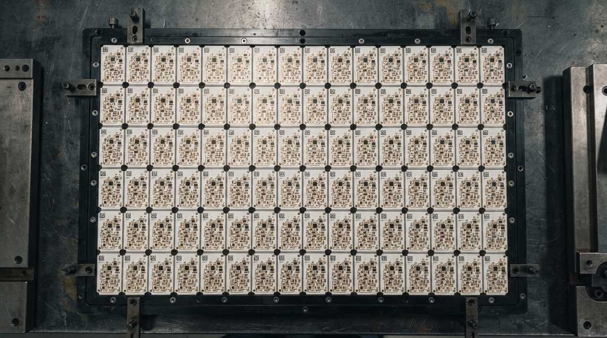
FR-4 fabricators typically print lot codes with inkjet or etch copper identifiers into a board edge. Neither method transfers directly to ceramic. Ink adhesion on alumina or aluminum nitride is poor without a glass frit binder, and most inks discolour or burn off during thick-film firing at 850 °C. Etched copper marks work only if the board has a copper layer in the marking zone, which wastes real estate on small substrates.
Ceramic substrates also tend to be smaller — often 10 × 10 mm to 50 × 50 mm per unit — so the marking footprint must be minimal. And because ceramic boards frequently enter high-temperature service environments above 200 °C, the mark itself must be thermally stable for the life of the product. These constraints make pcb traceability lot control on ceramics a distinct engineering problem.
Marking Methods Compared
| Method | Substrate compatibility | Min feature size | Survives reflow / wire bond | Typical use |
|---|---|---|---|---|
| Laser engraving (CO₂ or Nd:YAG) | Al₂O₃, AlN, Si₃N₄, ZrO₂ | ~50 µm line width | Yes — mark is ablated into the ceramic | Serial number, 2D Data Matrix |
| Thick-film screen print | Al₂O₃ (fired with circuit layers) | ~150 µm line width | Yes — co-fired glass/metal ink | Lot code, logo on large substrates |
| Inkjet (UV-cure) | Any, but adhesion varies | ~100 µm | No — degrades above ~260 °C | Temporary panel-level ID only |
| Label (polyimide) | Any flat surface | N/A | Survives reflow; not wire bond cleaning | Low-volume prototypes |
Typical values; confirm suitability with your process engineer for specific substrate grades and downstream assembly steps.
Laser engraving dominates production because the mark is physically part of the substrate. A Nd:YAG laser at 1064 nm ablates a shallow trench (5–20 µm deep) into the ceramic surface, producing a high-contrast mark on white alumina. On darker AlN substrates, contrast is lower; some fabs use a green (532 nm) frequency-doubled laser or apply a thin oxide witness layer first.
The marking step is typically performed after laser scribing of the ceramic panel but before singulation, so every unit receives its serial while still fixtured in the array.
What Data Fields Belong in a Ceramic PCB Lot Record
The physical mark on the board is just an index. The real pcb traceability lot control lives in your MES or quality database. A complete lot record for a ceramic PCB should include at minimum:
- Board serial number — unique per unit, encoded in the 2D Data Matrix on the substrate.
- Substrate lot — the supplier’s lot ID for the raw ceramic blank (e.g., Kyocera or Maruwa lot number), linking to the incoming inspection report and CoC.
- Paste / ink lot — for thick-film or DPC processes, the lot numbers of conductor paste, dielectric ink, and resistor paste.
- Firing profile ID — the specific furnace run, peak temperature, belt speed or dwell time, and atmosphere (air or N₂).
- Plating batch — if electroless Ni/Au or electrolytic plating is applied, the bath chemistry date and thickness measurement.
- Electrical test results — continuity, isolation, hi-pot values per board, linked to the serial.
- Visual / AOI inspection result — pass/fail with defect images if applicable.
- Operator and date stamps — for each major process step.
For aerospace builds per AS9100D, you also need to record any nonconformance dispositions (use-as-is, rework, scrap) against the serial. Medical device manufacturers working under 21 CFR Part 820 require the device history record (DHR) to trace back to the PCB lot.
Compliance Frameworks That Require PCB Traceability Lot Control
| Standard / regulation | Industry | Traceability requirement |
|---|---|---|
| IPC-6018 Class 3 | High-reliability electronics | Full forward and backward traceability of materials and processes |
| AS9100D §8.5.2 | Aerospace | Unique identification of product, traceability throughout realization |
| IATF 16949 §8.5.2 | Automotive | Lot traceability; 1-piece flow traceability for safety-critical parts |
| 21 CFR 820.184 | Medical devices (US) | Device history record linking each unit to production records |
| EU MDR Annex VI | Medical devices (EU) | UDI on or within the device; production traceability |
Each of these frameworks expects that a field failure can be traced backward through the entire production chain. A well-implemented pcb traceability lot control system makes that reverse lookup a database query rather than a forensic investigation.
Worked Example: Traceability Flow for a Ceramic Power Module Substrate
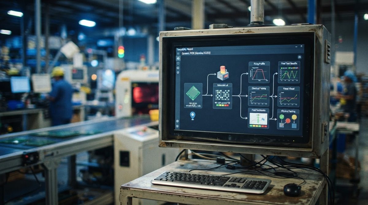
Consider a 25 × 30 mm DBC (direct bond copper) alumina substrate used in an automotive inverter. The IATF 16949–certified flow looks like this:
- Incoming 96% Al₂O₃ blanks arrive with the supplier’s lot certificate. The lot number is scanned into the MES at goods-in.
- During the ceramic PCB manufacturing process, each panel is assigned a panel ID linked to the substrate lot, copper foil lot, and bonding furnace run.
- After circuit patterning and etching, a Nd:YAG laser marks a 1.5 × 1.5 mm ECC 200 Data Matrix on each unit within the panel. The code encodes the serial number.
- Electrical test (continuity, hi-pot at 2.5 kV per IEC 60664-1) results are logged against each serial.
- X-ray inspection of internal vias confirms void percentage; the image file is stored against the serial.
- Finished boards ship with a lot summary and a CSV of serial-to-test-data mappings.
If a field failure occurs 5 years later, the customer scans the Data Matrix, retrieves the serial, and traces backward through every step to the raw alumina lot. This is pcb traceability lot control working as intended.
When Lot Traceability Is Not Worth the Cost
Unit-level serialization adds cost: laser marking time, MES integration, and data storage. For commodity LED boards or simple heater substrates sold in bulk without regulatory mandates, panel-level lot codes (one code per array, not per unit) are usually sufficient. If your end product does not face aerospace, automotive safety, or medical regulations, and your customer does not contractually require unit traceability, a simpler lot-level system saves money without meaningful risk.
Similarly, if your substrate is FR-4 or metal-core and you already have an established inkjet marking line, there is no reason to adopt laser marking — that method exists specifically because ceramic surfaces reject conventional inks.
Frequently Asked Questions
Can a laser mark damage the ceramic substrate electrically?
No. The ablation depth is typically 5–20 µm on a substrate that is 250–1000 µm thick. The mark does not penetrate to conductor layers or affect dielectric strength. Place the mark in a non-functional zone at least 0.5 mm from the nearest trace to avoid any risk of micro-cracking at the mark edge.
Do 2D Data Matrix codes survive soldering and wire bonding?
Yes. Because the code is ablated into the ceramic, it is unaffected by solder reflow (typically 260 °C peak) or thermosonic wire bonding (150–200 °C stage temperature). Codes remain readable after thermal cycling per IPC-TM-650 and even after exposure to the substrate’s full rated temperature.
What is the smallest area needed for a readable Data Matrix?
A 10 × 10 module ECC 200 symbol encoding a 10-character serial fits in approximately 1.5 × 1.5 mm with a 50 µm laser spot. Smaller codes are possible with finer lasers but may require higher-resolution scanners on the assembly line.
Is lot traceability required for prototype ceramic PCBs?
Not by regulation, but it is good practice. Prototypes often move into qualification builds. If you skip traceability at the prototype stage, you cannot later prove which substrate lot or firing profile produced the boards that passed qualification testing.
Can traceability data be embedded in a QR code instead of Data Matrix?
Technically yes, but Data Matrix (ECC 200) is the industry standard for small-part marking per IPC-1066 and SAE AS6496. QR codes require more area for the same data payload and are less common in pick-and-place scanner libraries.
Next Step
If your project requires unit-level serialization, specify it in your fabrication drawing or purchase order — including code format, location, and minimum module size. For more answers on ceramic substrate capabilities, browse the ceramic PCB frequently asked questions page.