PCB x-ray inspection uses transmitted radiation to image features that are invisible from the surface: buried vias, BGA solder balls, die-attach bond lines, and internal metallization. On ceramic substrates, x-ray is especially important because the high-Z ceramic body blocks optical inspection of anything below the top layer, and because void percentages in die-attach or via fills directly determine thermal resistance and long-term reliability.
Key Takeaways
- X-ray inspection detects voids, cracks, and misalignment in solder joints, via fills, and die-attach layers that no optical method can see.
- IPC-7095D limits voiding in BGA solder balls to ≤25% of the ball diameter area for Class 2 assemblies and ≤10% for Class 3.
- Die-attach void area above 5–10% measurably increases junction temperature; most power-device manufacturers specify ≤5% total void area.
- 2D x-ray is sufficient for single-layer ceramic boards; computed tomography (CT) is needed for multilayer ceramic PCB structures with stacked vias.
- X-ray adds cost per board but is far cheaper than a field failure caused by a hidden void in a power module.
How X-Ray Inspection Works on Ceramic Boards
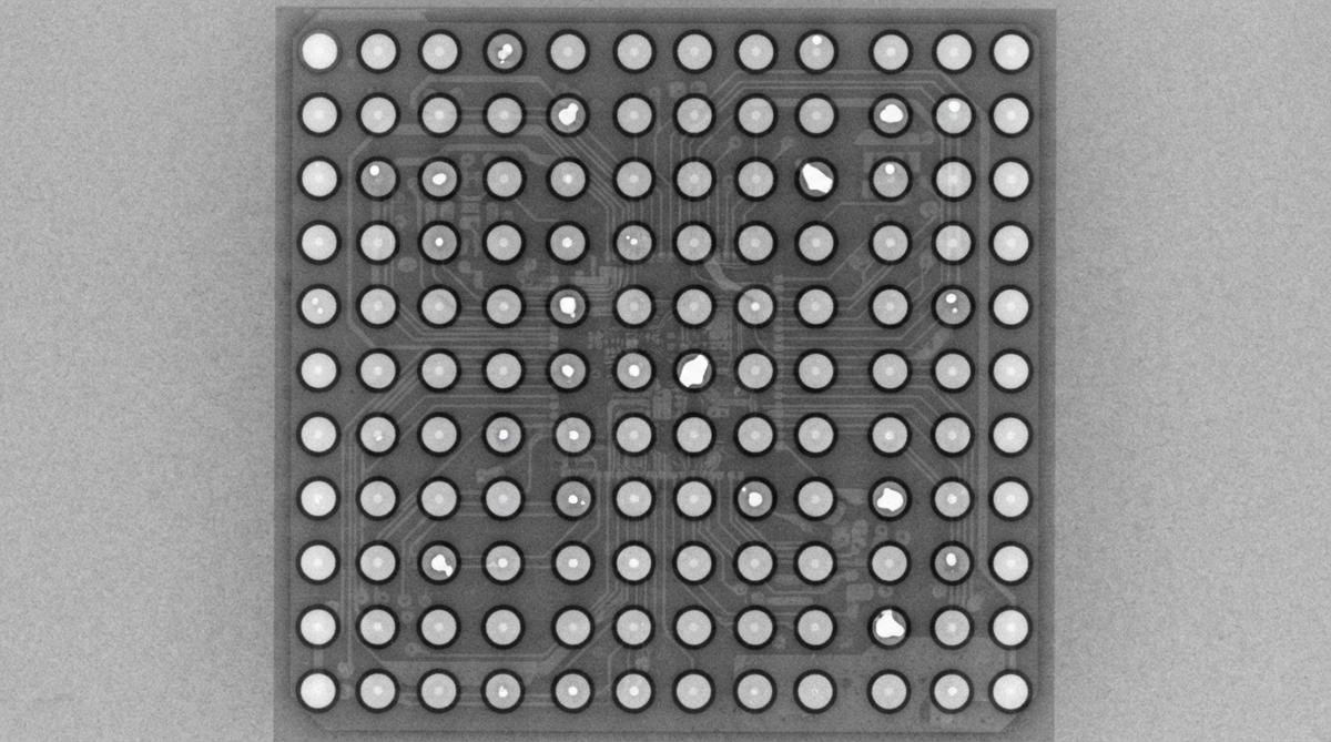
An x-ray tube generates a cone of radiation that passes through the board and hits a flat-panel detector or image intensifier on the other side. Dense materials (solder, copper, tungsten paste) absorb more x-rays and appear darker on the image; ceramic absorbs less and appears lighter. Voids—being air—appear as bright spots within a dark solder or metallization region.
Ceramic substrates present a specific challenge compared to FR-4. Alumina (Al₂O₃) has a higher atomic number and density than glass-epoxy, so the substrate itself absorbs more x-ray energy. This means you need a higher tube voltage (typically 90–130 kV for 0.635 mm alumina) and longer exposure times to get usable contrast on internal features. Aluminum nitride is slightly less absorbing, while ceramic substrate materials like zirconia are denser still and may require even higher kV settings.
2D Radiography vs. 3D Computed Tomography
Standard 2D x-ray produces a transmission image that collapses all layers into one plane. This works well for single-layer DBC or DPC boards where you only need to see one die-attach layer or one row of solder bumps. For multilayer HTCC or LTCC structures with buried vias at different depths, 2D images superimpose features and make void measurement unreliable. CT scanning rotates the sample through many angles and reconstructs a full 3D volume, letting you slice through any layer independently. CT is slower (minutes per sample versus seconds) and more expensive, but it is the only way to inspect stacked via chains inside a multilayer ceramic body.
What Defects X-Ray Catches That AOI Cannot
Automated optical inspection (AOI) examines the board surface. It catches missing components, tombstoned passives, solder bridges, and misaligned traces. But it is blind to anything beneath a component body or inside the substrate. The table below shows the division.
| Defect | AOI Detectable? | X-Ray Detectable? | Notes |
|---|---|---|---|
| Solder bridge (visible) | Yes | Yes | AOI is faster and cheaper for surface bridges |
| BGA solder ball void | No | Yes | Ball is hidden under component body |
| Head-in-pillow (BGA) | No | Yes | Partial collapse visible only in x-ray profile |
| Die-attach void | No | Yes | Bond line is under the die; acoustic microscopy is an alternative |
| Via fill void or crack | No | Yes | Critical for thermal vias in power substrates |
| Internal delamination | No | Partial | CT helps; C-SAM is better for planar delamination |
| Tombstoned passive | Yes | Yes | AOI is the standard tool here |
AOI and x-ray are complementary, not interchangeable. Most ceramic PCB production lines run AOI first, then x-ray on boards with hidden joints.
Enter your board details below to estimate what percentage of your joints require x-ray versus AOI-only coverage.
[pcb_calc type=”aoi-coverage”]
Accept/Reject Criteria for Common Hidden Features
Knowing what x-ray can see is only half the problem. You also need quantitative criteria for pass and fail. The numbers below come from IPC and device-manufacturer specifications.
BGA Solder Balls
Per IPC-7095D, a Class 2 (general electronics) BGA joint may have a void up to 25% of the ball cross-sectional area. Class 3 (high-reliability) tightens this to 10%. The void percentage is measured from the 2D x-ray image by dividing the bright area within the ball boundary by the total ball area. Multiple small voids are summed. A single void exceeding 10% of ball area in Class 3 is cause for rejection regardless of total count.
Die-Attach Bond Line
Die-attach voiding directly raises thermal resistance. A 10% void area in a solder die-attach can increase junction-to-case thermal resistance (RθJC) by 10–15%, per Infineon application note AN2019-03. Most power semiconductor datasheets specify ≤5% total void area, with no single void exceeding 2% of the die area. On ceramic substrates used for heat spreader designs, this limit is critical because the entire thermal path runs through the bond line.
Via Fills
Thermal and electrical vias filled with copper or tungsten paste must be inspected for trapped air. A common internal spec is ≤10% void area in the via cross-section. For thermal vias in power modules, tighter limits of ≤5% are typical. Cracks running the length of a via are always a reject, regardless of void percentage, because they create a thermal discontinuity that worsens under thermal cycling.
Worked Example: Void Impact on Thermal Resistance
Suppose you have a 5 × 5 mm silicon die soldered to a 96% alumina substrate (24 W/m·K) with a 25 µm thick SAC305 solder bond line (k ≈ 58 W/m·K). The thermal resistance of the bond line alone, assuming zero voids:
Rth,bond = t / (k × A) = 0.000025 / (58 × 0.000025) = 0.017 °C/W
Now assume 10% voiding. Voids are air (k ≈ 0.026 W/m·K), so the effective area for conduction drops to 90% of the die area. The voided region contributes almost no conduction. Effective Rth rises to approximately 0.019 °C/W—an 12% increase. At 50 W dissipation, that is roughly 0.1 °C extra at the junction. Sounds small, but stack this with a partially voided thermal via array and cumulative thermal resistance climbs fast. At 200 W, the same 10% voiding costs 0.4 °C, and in a power module with tight thermal margins, that can push the junction past its rated limit.
When X-Ray Is Mandatory vs. Optional
X-ray inspection is not free. A 2D x-ray station costs $150k–$400k; CT systems run $500k–$1.5M. Per-board inspection time adds cost to every unit. Use x-ray when the return justifies it:
- Mandatory: Any board with BGA, LGA, or QFN packages (hidden solder joints). Any die-attach bond line in a power or RF module. Any filled via array carrying thermal load. Any Class 3 / IPC-6012 Class 3/A assembly.
- Recommended: First article inspection on new ceramic designs, even if production will rely on process controls. Boards going into medical, automotive, or aerospace end-use where field failure cost is high.
- Optional: Simple single-sided ceramic boards with only surface-mount passives and visible joints. Here AOI alone is sufficient and x-ray adds cost without meaningful yield improvement.
When Not to Use X-Ray
X-ray is the wrong tool if your defect is on the surface. Solder paste height, component polarity, and marking legibility are faster and cheaper to inspect with AOI or manual optical microscopy. X-ray also struggles with planar delamination in multilayer ceramics; scanning acoustic microscopy (C-SAM) is more sensitive for that failure mode. If your ceramic board has only through-hole or exposed-pad components with no hidden joints, x-ray adds inspection cost with no quality benefit. Spend the budget on thermal simulation instead to catch design-level thermal problems before fabrication.
Frequently Asked Questions
Does x-ray inspection damage ceramic PCBs?
No. The x-ray doses used in PCB inspection (typically <1 Gy per exposure) are far below the threshold for radiation damage to ceramics, metals, or solder alloys. Sensitive ICs are also safe at these dose levels, per JEDEC JESD22-A108.
Can x-ray measure the thickness of a die-attach layer?
Standard 2D x-ray cannot measure bond-line thickness accurately because it produces a plan-view image. CT scanning can reconstruct a cross-section and measure thickness to within ±5 µm, depending on voxel resolution. For production-line thickness checks, a cross-section or acoustic microscopy is more common.
How long does x-ray inspection take per board?
A single 2D image takes 2–10 seconds depending on board size and required resolution. Automated void analysis software adds another 1–3 seconds per region of interest. A full CT scan of a 25 × 25 mm ceramic substrate takes 5–20 minutes, making CT impractical for 100% production inspection but standard for sampling and failure analysis.
Is x-ray required by IPC standards for ceramic PCBs?
IPC-6012 does not mandate x-ray for all ceramic boards. However, IPC-7095D effectively requires x-ray or equivalent for any BGA assembly, and IPC-A-610 Class 3 assemblies with hidden joints must be inspected by a method capable of detecting internal voids. X-ray is the de facto method that satisfies both requirements.
What x-ray resolution do I need for ceramic via inspection?
A feature resolution (detector pixel size) of 10–20 µm is sufficient for vias ≥100 µm diameter. For fine-pitch vias below 100 µm, such as those in LTCC structures, you need ≤5 µm resolution, which typically requires a micro-focus x-ray source. Check that your inspection house can achieve the resolution your via geometry demands.
Next Step
If your ceramic board has hidden solder joints, filled vias, or die-attach layers, specify x-ray inspection in your fabrication drawing and define void acceptance criteria before production starts. Review the full ceramic PCB FAQ for related quality and inspection topics, or request a quote that includes x-ray inspection as part of the inspection flow.