A thermal shock test PCB qualification subjects the assembly to rapid, repeated temperature swings—typically between –55 °C and +125 °C or wider—to expose latent defects in solder joints, metallization adhesion, via integrity, and substrate cohesion before the board reaches the field. Thermal cycling tests use the same temperature extremes but at slower ramp rates. Both are accelerated-life methods that compress years of service into days or weeks on the bench. Understanding how a thermal shock test PCB protocol works is essential for any engineer qualifying ceramic or organic boards for harsh environments.
Key Takeaways
- A thermal shock test PCB profile uses transfer times under 20 seconds between hot and cold zones; thermal cycling allows 10–20 °C/min ramps per IPC-9701A.
- The dominant failure mode in organic PCBs is solder-joint fatigue driven by CTE mismatch; ceramic substrates reduce this mismatch for bare-die attach.
- 96% alumina survives >1 000 cycles at –55 °C to +150 °C without substrate cracking, per CoorsTek ADS-996 data.
- MIL-STD-883 Method 1010 and IEC 60068-2-14 (Test Na/Nb) are the two most-referenced thermal shock standards for electronics.
- Coffin–Manson modelling lets you convert accelerated-test cycles to field-life estimates once you know the temperature swing ΔT and the fatigue exponent.
Thermal Shock Test PCB vs. Thermal Cycling: What Is the Difference?
Engineers sometimes use the terms interchangeably, but the standards draw a clear line. Thermal shock imposes an abrupt temperature change—the board moves between hot and cold zones in seconds. Thermal cycling ramps the temperature at a controlled rate, holds it at each extreme (a dwell), and repeats. The distinction matters because the stress profile is different: shock generates steep thermal gradients through the board thickness, while cycling allows the assembly to reach near-equilibrium at each extreme, stressing solder joints and interfaces through bulk CTE mismatch rather than transient gradients.
For ceramic PCBs, the transient gradient during shock is especially relevant. Ceramics have lower thermal diffusivity than copper-clad FR-4, so a thick alumina substrate can develop internal tensile stress if the surface cools faster than the core. Thin substrates (≤0.635 mm) are far less susceptible. Designers working with alumina 96% thermal design rules should account for substrate thickness when selecting a thermal shock test PCB profile.
Major Test Standards at a Glance
| Standard | Method | Type | Typical Profile | Transfer / Ramp | Common Cycle Count |
|---|---|---|---|---|---|
| MIL-STD-883 | 1010, Cond. B | Shock (air-to-air) | –55 °C to +125 °C | < 10 s transfer | 100–500 |
| MIL-STD-883 | 1010, Cond. C | Shock (air-to-air) | –65 °C to +150 °C | < 10 s transfer | 100–500 |
| IEC 60068-2-14 | Test Na (rapid) | Shock (liquid or air) | Per spec, e.g. –40 °C to +125 °C | < 20 s transfer | 10–200 |
| IEC 60068-2-14 | Test Nb (gradual) | Cycling | Per spec | 1–5 °C/min | Per spec |
| IPC-9701A | TC1 / TC2 / TC3 | Cycling | 0 °C to +100 °C / –40 to +125 °C / –55 to +125 °C | 10–20 °C/min, 10 min dwell | 3 000–6 000 |
| JEDEC JESD22-A104 | Cond. G | Cycling | –40 °C to +125 °C | 10–15 °C/min | 500–1 000 |
| AEC-Q100 | Test A | Cycling | –40 °C to +125 °C (Grade 1) | Per JESD22-A104 | 1 000 |
Typical values for commercially available test profiles, for comparison only. Confirm against the current revision of each standard for your specific qualification.
How a Thermal Shock Test PCB Qualification Is Actually Run
- Pre-test inspection. Record baseline resistance of daisy-chain or continuity coupons. Perform X-ray inspection of vias and die-attach if the DUT includes hidden joints.
- Chamber setup. For air-to-air shock, two chambers are held at Tmin and Tmax. A transfer mechanism (basket or elevator) moves the boards between zones. For liquid-to-liquid, fluorinated fluids (e.g., 3M Fluorinert FC-77 at –65 °C and FC-40 at +150 °C) provide faster heat transfer.
- Cycling. The board dwells at each extreme long enough to reach thermal equilibrium—typically 5–15 minutes depending on mass. Transfer time must stay under the standard’s limit (often 10–20 s).
- Interim reads. Every 100 or 250 cycles, measure continuity. A >20% resistance increase or an open circuit is a failure per IPC-9701A.
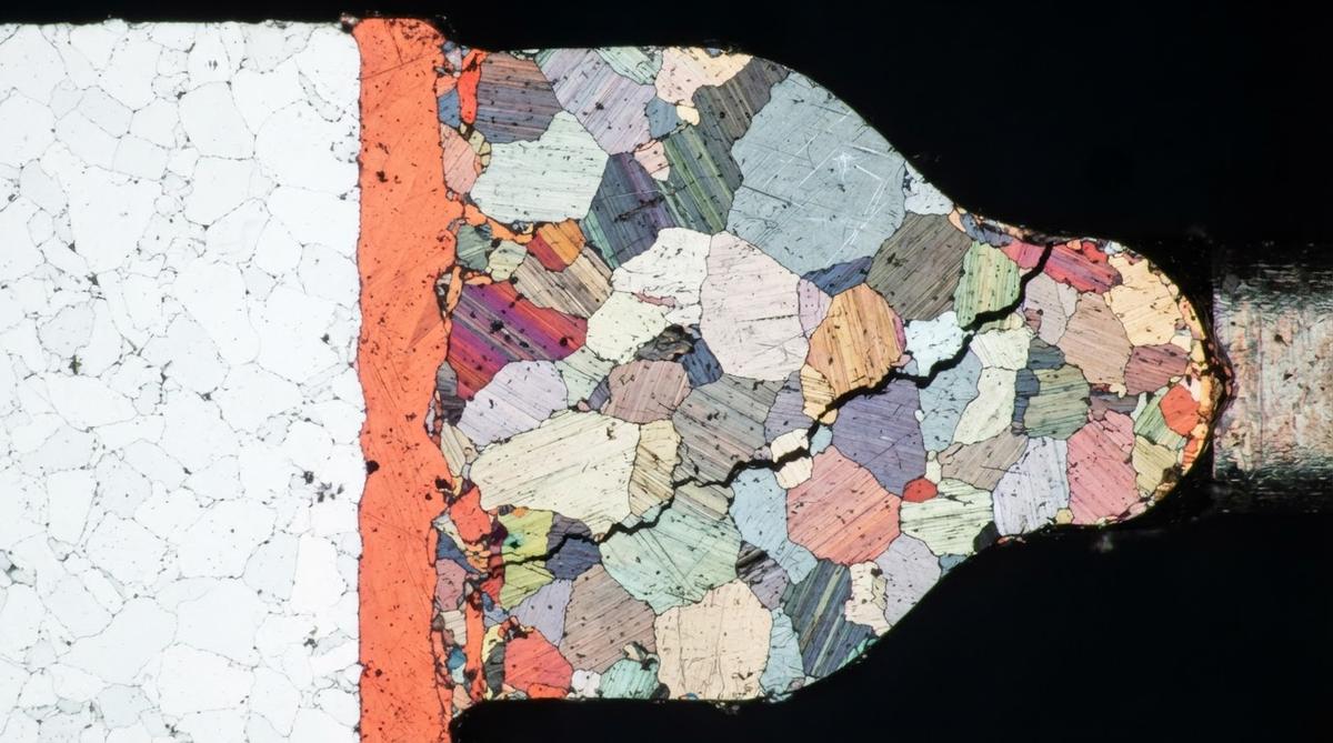
- Post-test analysis. Cross-section suspect joints. Look for solder fatigue cracks, pad cratering, via barrel cracks, or delamination. On ceramic boards, inspect for substrate micro-cracks under polarized light.
Why Ceramic Substrates Survive More Thermal Shock Test PCB Cycles
The primary driver of solder-joint fatigue during thermal cycling is the CTE mismatch between the substrate and the component (typically a silicon die at ~3 ppm/°C). FR-4 has a CTE of 14–17 ppm/°C in-plane and 50–70 ppm/°C through-thickness. 96% alumina sits at 6.5–7.2 ppm/°C (per CoorsTek ADS-996 datasheet, ASTM E228), and aluminum nitride at 4.5–5.0 ppm/°C—much closer to silicon. This smaller mismatch means lower cyclic shear strain on the solder, which directly extends fatigue life according to the Coffin–Manson relation.
For boards operating across extreme temperature ranges, the maximum operating temperature of a ceramic PCB can exceed 350 °C for the substrate itself, though metallization and solder set the practical ceiling. Silicon nitride (Si₃N₄) adds another advantage: its flexural strength of 600–900 MPa (per Kyocera SN series datasheet, ASTM C1161) resists crack initiation under shock far better than alumina’s 300–380 MPa. For more on Si₃N₄ properties, see the silicon nitride thermal conductivity guide.
Worked Example: Coffin–Manson Cycle-Life Estimate
The Coffin–Manson equation for solder-joint fatigue life is:
Nf = C · (Δγ)–n
where Nf is cycles to failure, Δγ is the cyclic shear strain range, and C and n are material constants (for SAC305 solder, n ≈ 1.9–2.2 per Syed’s model, ASME Journal of Electronic Packaging, 2004).
Shear strain Δγ ≈ (Δα · ΔT · L) / h, where Δα is the CTE difference, ΔT is the temperature swing, L is the distance from the neutral point to the farthest solder joint, and h is the solder-joint standoff height.
Scenario: 10 mm × 10 mm BGA on FR-4 vs. 96% Alumina
Assume ΔT = 165 °C (–40 °C to +125 °C), L = 7.07 mm (half-diagonal), h = 0.5 mm, component CTE = 6 ppm/°C.
- FR-4: Δα = 16 – 6 = 10 ppm/°C → Δγ = (10 × 10⁻⁶ × 165 × 7.07) / 0.5 = 0.0233 (2.33%)
- 96% Al₂O₃: Δα = 7 – 6 = 1 ppm/°C → Δγ = (1 × 10⁻⁶ × 165 × 7.07) / 0.5 = 0.00233 (0.23%)
Using n = 2.0 and a constant C calibrated so the FR-4 case gives Nf = 800 cycles (a typical IPC-9701A TC2 result for 0.5 mm-pitch BGA on FR-4):
Nf,ceramic / Nf,FR-4 = (ΔγFR-4 / Δγceramic)2.0 = (0.0233 / 0.00233)2 = 100
The alumina board would reach roughly 80 000 cycles to first failure under the same thermal shock test PCB profile—about 100× the FR-4 life. Real-world results will be lower due to metallization fatigue, pad geometry, and voiding, but the order-of-magnitude advantage is consistent with published data.
Enter your own substrate CTE, temperature range, and joint geometry below to compare cycle-life estimates across different substrates.
[pcb_calc type=”thermal-cycling”]
Common Failure Modes by Substrate Type
| Failure Mode | FR-4 / Organic | 96% Alumina | AlN | Si₃N₄ (AMB) |
|---|---|---|---|---|
| Solder-joint fatigue crack | Primary failure | Rare (low Δα) | Rare (low Δα) | Rare (low Δα) |
| Pad cratering / lift | Common above 2 000 cycles | Not applicable | Not applicable | Not applicable |
| Via barrel crack | Common (Z-axis CTE) | Very rare | Very rare | Very rare |
| Substrate cracking | Not typical | Possible if > 1 mm thick + rapid shock | Possible | Highly resistant |
| Copper delamination | Possible (resin degradation) | DBC: possible at Cu/ceramic interface after > 3 000 wide-ΔT cycles | AMB: very resistant | AMB: very resistant |
| Delamination / blistering | Common above Tg | Not applicable | Not applicable | Not applicable |
Qualitative comparison based on published reliability literature. Actual performance depends on design, process, and specific material grade.
When NOT to Use Thermal Shock Testing
Thermal shock is not always the right qualification method. If your product operates in a benign environment (indoor commercial electronics, ΔT < 40 °C), IPC-9701A TC1 cycling (0 °C to +100 °C) is more representative and less likely to introduce failure modes your product will never see. Running MIL-STD-883 Cond. C on a consumer wearable wastes chamber time and may drive unnecessary design changes.
Likewise, if the primary reliability concern is humidity or electrochemical migration rather than thermo-mechanical fatigue, an 85 °C / 85% RH test (JEDEC JESD22-A101) is a better use of your test budget. A thermal shock test PCB protocol tells you about mechanical integrity—it tells you nothing about corrosion, dendritic growth, or insulation resistance degradation.
For boards where ceramic thermal management is the design driver but the operating environment is stable (e.g., a laser diode in a temperature-controlled enclosure), a handful of qualification cycles may suffice. Spend your reliability budget on the failure mode most likely to occur in the actual use case.
Frequently Asked Questions
How many thermal shock cycles should I specify for a ceramic PCB?
For mil/aero applications, 100–500 cycles at –55 °C to +125 °C per MIL-STD-883 Method 1010 is standard. For automotive power modules, AEC-Q100 Grade 1 requires 1 000 cycles at –40 °C to +125 °C. Ceramic substrates routinely pass these counts without substrate failure; the limiting factor is usually the copper-to-ceramic bond in DBC or the solder joint.
Does liquid-to-liquid shock damage ceramic boards?
It can, but only under specific conditions. Thin substrates (≤0.635 mm) tolerate liquid-to-liquid shock well because the thermal gradient through the thickness stays small. Thicker substrates or those with existing edge micro-cracks are more vulnerable. If you must use liquid shock on a thick ceramic board, inspect edges under magnification before and after testing.
Can I compare thermal cycling data between different standards?
Not directly. IPC-9701A uses slow ramps and long dwells, while MIL-STD-883 uses rapid transfer. The dwell time affects creep relaxation in the solder, which changes the effective strain range per cycle. You can use acceleration-factor models (Norris–Landzberg) to convert between profiles, but the conversion introduces uncertainty of ±20–30%.
What is the pass/fail criterion for thermal cycling per IPC-9701A?
A daisy-chain net fails when its resistance increases by more than 20% from the initial value, or when an open circuit (resistance > 500 Ω for > 1 µs) is detected during continuous monitoring. The board-level criterion is typically defined as the cycle count at which the first 1% of joints fail (N1%), characterized using Weibull statistics.
Do I need traceability for thermal shock test PCB coupons?
Yes, especially for aerospace and automotive qualification. Each coupon should be traceable to a specific production lot, substrate batch, and solder paste lot. Proper lot traceability and serialization lets you correlate any field failure back to manufacturing variables.
Next Step
If you are designing a ceramic board that must survive a specific thermal shock test PCB qualification, start by reviewing the maximum operating temperature limits for your chosen substrate material, then select a metallization system that matches your reliability target. To discuss test requirements or request a quote for boards built to your qualification spec, visit the ceramic PCB FAQ hub or contact our engineering team directly.