Ceramic PCB quality control is a gate-by-gate inspection sequence that runs from incoming substrate verification through final outgoing screening, typically spanning eight or more discrete checkpoints. Every gate has defined test methods, accept/reject criteria, and documentation requirements. Skip or compress any gate and you risk shipping boards with latent defects that surface only after assembly or in the field.
This article maps the full QC flow, names the specific tests at each stage, and gives the pass/fail criteria engineers should write into purchase specifications.
Why Ceramic PCBs Need a Dedicated QC Flow
FR-4 fabrication tolerates some variation because the laminate is forgiving: it flexes, it absorbs minor registration errors, and rework is often possible. Ceramic substrates are brittle, expensive per unit area, and frequently destined for power electronics, RF modules, or medical implants where field failure is unacceptable. A micro-crack invisible to the naked eye can propagate under thermal cycling and cause an open circuit months later.
The cost profile also changes the math. Ceramic substrate material alone can represent 30–60% of finished board cost depending on grade (Al₂O₃ 96% vs. AlN vs. Si₃N₄). Catching a defective substrate before metallization saves the full processing cost downstream. That economic reality drives the inspection-heavy flow described below.
Yield management ties directly into QC discipline. For a deeper look at what drives scrap rates, see ceramic PCB yield and scrap rate drivers.
The Eight-Gate Ceramic PCB QC Flow
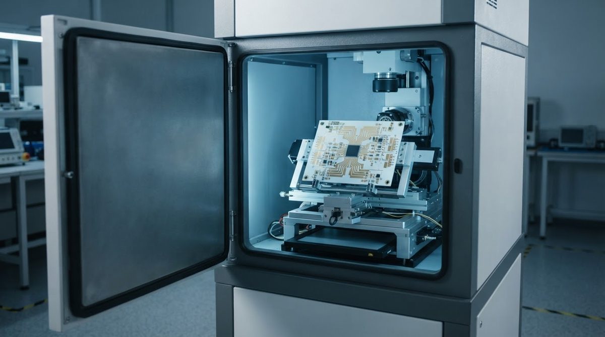
The sequence below represents a typical production flow. Some facilities combine adjacent gates or add extras for specific applications (e.g., wire-bond pull testing for die-attach boards). The core logic is universal: inspect before you add value, and inspect again after each irreversible process step.
Gate 1 — Incoming Substrate Inspection
Every lot of blank ceramic substrates is checked before entering production. Key checks include dimensional verification (length, width, thickness, and warpage and flatness per the drawing), visual inspection under 10× magnification for edge chips, surface pits, and cracks, and a sample dielectric strength test. Substrates that exceed the warpage limit (commonly ≤ 0.1 mm per 25.4 mm for thin substrates) are rejected or downgraded.
Lot traceability starts here. Each incoming lot gets a unique identifier that follows it through every subsequent gate. For details on how serialization works in practice, see lot traceability and serialization on ceramic PCBs.
Gate 2 — Post-Metallization Visual and Dimensional
After thick-film screen printing, thin-film sputtering, or DPC/DBC copper processing, the metallized pattern is inspected. AOI (automated optical inspection) checks trace width, space, and registration against Gerber data. Dimensional tolerances for trace width are typically ±10–25 µm depending on the process (DPC tighter, thick film wider). Any bridging, opens, or pattern shift beyond tolerance triggers reject.
Gate 3 — Electrical Continuity and Isolation
Flying-probe or fixture-based testing confirms every net is continuous and no unintended shorts exist. Isolation resistance between adjacent conductors is measured at a specified voltage (often 100 V DC for low-voltage designs, higher for power boards). A typical pass criterion is ≥ 100 MΩ isolation resistance and ≤ 50 mΩ continuity resistance per net, though these values depend on the design.
Gate 4 — Dielectric Withstand (Hipot)
For power electronics and high-voltage applications, a dielectric withstand test on ceramic PCBs is performed per IEC 60664 or the customer’s specification. A voltage is applied between isolated conductors (or between a conductor and the substrate backside) and held for 60 seconds. Typical test voltages range from 1.5 kV to 10 kV AC depending on the rated working voltage. Any breakdown or leakage current above the specified limit (often 1 mA) is a hard reject.
Gate 5 — X-Ray Inspection (Where Applicable)
Boards with filled vias, buried conductors, or brazed metal layers require X-ray inspection of internal vias and joints. X-ray reveals voids in via fills (accept limit often ≤ 25% void area per IPC-6012), delamination at DBC/AMB copper-ceramic interfaces, and misalignment of internal features. This gate is mandatory for automotive and aerospace builds; it may be sample-based for commercial-grade orders.
Gate 6 — Solderability Testing (Sample)
A sample from each lot undergoes solderability testing per IPC J-STD-003 or equivalent. The surface finish (ENIG, ENEPIG, bare copper + OSP, etc.) must wet within the specified time and coverage threshold, typically ≥ 95% wetting area. Boards that fail solderability testing indicate a process drift in plating or surface finish that must be corrected before the lot ships. More on this at solderability testing for ceramic substrates.
Gate 7 — Environmental and Reliability Screening (Sample or 100%)
Depending on the application class, a sample set undergoes thermal shock or thermal cycling per IPC-TM-650 or MIL-STD-883. A common ceramic PCB thermal shock profile is −40 °C to +150 °C for 100–500 cycles, with post-test electrical and visual re-inspection. Boards are also checked for adhesion (tape-peel test per ASTM D3359, expecting no lift at Class 5B) and, for wire-bond pads, bond-pull strength. For a full treatment of thermal shock methods, see thermal shock and thermal cycling test methods.
Gate 8 — Final Outgoing Inspection and Packaging
Every board gets a final visual inspection under 10–30× magnification against the acceptance criteria in IPC-A-600 Class 2 or Class 3 (as specified by the customer). Dimensional spot checks confirm the board still meets drawing tolerances after all processing. Boards are then packaged in ESD-safe, moisture-barrier bags with desiccant for shipment.
Inspection Methods and Criteria at a Glance
| QC Gate | Method | Key Standard | Typical Accept Criterion |
|---|---|---|---|
| Incoming substrate | CMM, optical profilometer, visual | Customer drawing, ASTM C1161 | Warpage ≤ 0.1 mm/25.4 mm; no edge chips > 0.2 mm |
| Post-metallization | AOI, microscope | IPC-A-600 Class 2/3 | Trace width ±10–25 µm; no bridging or opens |
| Electrical test | Flying probe / fixture | IPC-9252 | Continuity ≤ 50 mΩ; isolation ≥ 100 MΩ @ 100 V DC |
| Hipot | Dielectric withstand tester | IEC 60664, UL 60950 | No breakdown at rated test voltage; leakage < 1 mA |
| X-ray | 2D/3D X-ray | IPC-6012 | Via void area ≤ 25% |
| Solderability | Dip-and-look or wetting balance | IPC J-STD-003 | ≥ 95% wetting coverage |
| Thermal shock | Thermal shock chamber | IPC-TM-650, MIL-STD-883 | No cracks, no resistance change > 10% after 100+ cycles |
| Final outgoing | Visual 10–30×, CMM spot check | IPC-A-600 Class 2/3 | Per customer drawing and IPC acceptance criteria |
Typical values for commercially available processes, for comparison only. Confirm against your supplier’s quality plan and your own acceptance specification.
First Article Inspection: The Gate Before Production
Before full production begins on a new part number, a First Article Inspection (FAI) validates that the process can produce boards meeting all drawing requirements. The FAI report documents every measured dimension, every electrical test result, and every material certification against the design specification. It is a contractual deliverable for aerospace (AS9102) and automotive (PPAP) programs, and good practice even for commercial builds. A thorough FAI catches tooling errors, registration offsets, and material substitutions before they propagate across an entire lot. Details on what a ceramic PCB FAI report should contain are covered in first article inspection for ceramic PCBs.
Worked Example: Specifying QC in a Purchase Order
Suppose you are ordering 500 pieces of a 25 mm × 25 mm AlN DPC board for a power module. Your PO should specify, at minimum:
- Acceptance class: IPC-A-600 Class 3 (high reliability).
- Hipot requirement: 5 kV AC for 60 s, leakage < 0.5 mA.
- Thermal shock sample: 5 pieces per lot, −55 °C to +150 °C, 200 cycles, post-test electrical re-test.
- X-ray: 100% inspection on via fills, void limit ≤ 20%.
- Solderability: Sample per IPC J-STD-003, ≥ 95% wetting.
- FAI: Full dimensional and electrical report per AS9102 on the first 3 pieces.
- Traceability: Lot code laser-marked on each board; CoC with lot-level test data.
Writing these requirements explicitly prevents the supplier from defaulting to a lower inspection level and gives you audit rights if boards fail in assembly.
When QC Alone Is Not Enough
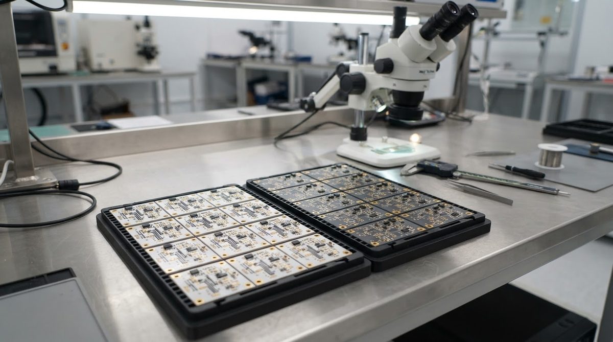
Quality control catches defects. It does not prevent them. If your yield is consistently below 85%, adding more inspection gates will not fix the root cause. The right move is a process capability study (Cpk analysis) on the failing parameter, followed by process correction. QC data should feed back into process control; if it only feeds forward into sort-and-ship, you are paying for inspection without getting improvement.
Similarly, if your application is commercial IoT or consumer LED and your volumes exceed a few thousand pieces, the cost of 100% X-ray and thermal shock screening may not be justified. For those builds, AQL-based sampling (e.g., AQL 1.0, Level II per ISO 2859-1) gives statistical confidence at a fraction of the cost. Reserve 100% screening for Class 3 applications where a single field failure has safety or mission consequences.
When Not to Use Ceramic — and When to Relax QC
If your board operates below 130 °C, carries no high-voltage isolation requirement, and does not need CTE matching to a semiconductor die, FR-4 or metal-core PCB may be the better choice. Standard FR-4 QC flows are well-established, faster, and cheaper. The elaborate QC flow described above exists because ceramic substrates serve applications where the consequences of failure justify the cost of inspection. If that does not describe your project, the substrate choice itself may be wrong.
Even within ceramic, not every board needs every gate. A prototype run of 10 pieces for bench evaluation does not need 200-cycle thermal shock screening. Match the QC depth to the program phase and the reliability requirement.
Frequently Asked Questions
What standards govern ceramic PCB quality control?
IPC-A-600 (acceptability of printed boards), IPC-6012 (qualification and performance specification), IPC J-STD-003 (solderability), and IEC 60664 (insulation coordination) are the most commonly referenced. Aerospace programs add AS9102 for FAI and AS9100D for the quality management system. Military applications may invoke MIL-PRF-55342 or MIL-STD-883 for specific tests.
Is 100% inspection standard for ceramic PCBs?
Visual inspection and electrical testing are typically 100% for ceramic boards due to the high unit cost and reliability requirements. Destructive or semi-destructive tests (thermal shock, cross-section, bond pull) are sample-based. X-ray may be 100% or sample-based depending on the application class and customer specification.
How do I verify my supplier’s QC process?
Request the supplier’s quality plan or control plan for your specific part number. It should list every inspection gate, the method, the acceptance criterion, the sample size, and the recording method. An on-site audit or a third-party audit (per ISO 9001 or IATF 16949) provides additional assurance. At minimum, require a Certificate of Conformance with lot-level test data for each shipment.
Can AOI catch micro-cracks in ceramic substrates?
Standard AOI detects surface-level pattern defects (opens, shorts, registration errors) but is unreliable for subsurface micro-cracks in the ceramic body. Fluorescent dye penetrant inspection or acoustic microscopy (C-SAM) is more effective for crack detection. X-ray can reveal cracks that have propagated enough to create a measurable gap.
What is a typical AQL for ceramic PCB lots?
AQL 0.65 to 1.0 at General Inspection Level II (per ISO 2859-1) is common for Class 3 ceramic boards. Commercial-grade boards may use AQL 1.0 to 2.5. The AQL applies to the sampling-based gates (solderability, thermal shock); 100%-inspected gates do not use AQL sampling since every unit is checked.
Next Step
If you are writing a ceramic PCB specification or evaluating a supplier’s QC capability, the reliability screening and test overview provides additional context on individual test methods. For questions about a specific project, request a quote and ask for the proposed quality plan alongside pricing.