Silicon nitride Si3N4 DBC direct bonded copper substrates pair the toughest structural ceramic used in electronics with a Cu–O eutectic metallization process. The result is a substrate that survives thermal cycling regimes that crack alumina and aluminum nitride alternatives—typically rated for 3,000+ cycles between −40 °C and +250 °C per JEDEC JESD22-A104 without copper delamination. That durability comes at a cost premium of roughly 3–5× over Al2O3 DBC and 1.5–2.5× over AlN DBC, so silicon nitride Si3N4 DBC direct bonded copper technology earns its place only in high-reliability power electronics.
Key Takeaways
- Si3N4 substrates reach a fracture toughness of 6–7 MPa·√m (per Kyocera SN series datasheet, ASTM E1820), roughly 3× that of 96% alumina and 5× that of AlN.
- Thermal conductivity of Si3N4 ranges from 70–90 W/mK for high-thermal grades (Toshiba, CeramTec), lower than AlN (170–200 W/mK) but adequate for most power-module geometries.
- DBC copper thickness on Si3N4 is typically 0.15–0.50 mm; thicker copper increases current capacity but raises thermomechanical stress during bonding.
- Primary applications: EV traction inverters, railway IGBT modules, and aerospace power converters where thermal-cycle life defines field reliability.
- Silicon nitride Si3N4 DBC direct bonded copper assemblies are not cost-effective for designs under 1,000 thermal cycles or junction temperatures below 150 °C—use alumina DBC instead.
What Is Silicon Nitride Si3N4 DBC Direct Bonded Copper?
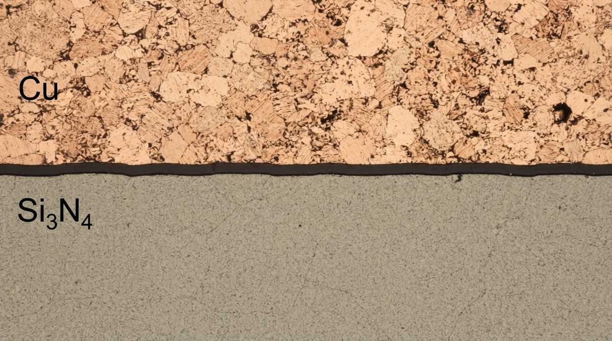
DBC (direct bonded copper) is a process that bonds a copper foil to a ceramic substrate using a controlled Cu–O eutectic layer formed at approximately 1,065 °C in a nitrogen-oxygen atmosphere. The copper sheet oxidizes slightly at the interface, creating a thin CuO–Cu₂O film that wets the ceramic surface and forms a permanent bond upon cooling. The process applies to Al2O3, AlN, and Si3N4 substrates, but the ceramic’s mechanical properties determine how well the finished assembly tolerates repeated thermal stress.
Silicon nitride’s advantage is its combination of high flexural strength (600–900 MPa per ASTM C1161, four-point bend) and high fracture toughness. When copper expands and contracts during power cycling, the ceramic must absorb tensile stress at the bond interface without initiating cracks. Si3N4 handles this far better than alumina (300–400 MPa) or AlN (300–350 MPa). You can verify copper peel strength on ceramic substrates to understand how bond integrity is measured across different ceramic types.
Silicon Nitride Si3N4 DBC Direct Bonded Copper vs. Al2O3 and AlN DBC
| Parameter | Si3N4 (high-thermal grade) | AlN | Al2O3 96% | Unit | Condition / Source |
|---|---|---|---|---|---|
| Thermal conductivity | 70–90 | 170–200 | 24–28 | W/mK | 20 °C; Kyocera SN series, CoorsTek datasheets |
| Flexural strength | 600–900 | 300–350 | 300–400 | MPa | ASTM C1161, 4-pt bend |
| Fracture toughness | 6–7 | 2.5–3.0 | 3.5–4.0 | MPa·√m | ASTM E1820 |
| CTE (25–400 °C) | 2.7–3.2 | 4.5–5.0 | 7.0–8.0 | ppm/K | Manufacturer datasheets |
| Dielectric strength | 15–18 | 14–17 | 10–15 | kV/mm | IEC 60243-1 |
| Typical DBC Cu thickness | 0.15–0.50 | 0.15–0.50 | 0.15–0.40 | mm | Industry standard |
| Thermal-cycle life (−40/+250 °C) | >3,000 | 500–1,500 | 200–800 | cycles to delamination | JEDEC JESD22-A104 |
| Relative substrate cost | 3–5× | 1.5–2.5× | 1× (baseline) | — | Market pricing, 2024 |
Typical values for commercially available material, for comparison only. Confirm against the datasheet for your specific grade.
Why Thermal-Cycle Life Matters More Than Thermal Conductivity
Engineers often default to AlN for power modules because its thermal conductivity is roughly double that of Si3N4. In a simple steady-state calculation, AlN wins. But power modules in traction inverters or railway converters do not operate at steady state—they cycle between ambient and 175–250 °C junction temperatures thousands of times over a 15–30 year service life.
Consider a worked example. An IGBT module dissipates 150 W across a 30 × 30 mm substrate, 0.32 mm thick. Steady-state thermal resistance through the ceramic alone:
- AlN (180 W/mK): Rth = t / (k × A) = 0.00032 / (180 × 0.0009) = 0.00198 K/W → ΔT ≈ 0.30 °C
- Si3N4 (80 W/mK): Rth = 0.00032 / (80 × 0.0009) = 0.00444 K/W → ΔT ≈ 0.67 °C
The difference is 0.37 °C—negligible compared to the solder-layer and heat-sink thermal resistances that dominate the stack. Meanwhile, if the AlN substrate cracks at cycle 800 and the Si3N4 substrate survives past cycle 3,000, the thermal-conductivity advantage is irrelevant. For designs where cycle life is the binding constraint, silicon nitride Si3N4 DBC direct bonded copper is the correct choice despite lower k.
Enter your substrate area, thickness, and dissipated power below to estimate junction temperature rise for different ceramic materials.
DBC Process Considerations for Si3N4
Bonding copper to Si3N4 is more demanding than bonding to alumina. Si3N4 has a lower CTE (2.7–3.2 ppm/K vs. copper’s ~17 ppm/K), creating higher residual stress after cool-down from the bonding temperature. Manufacturers address this by controlling copper thickness—thinner foils reduce stress—and by optimizing the oxidation atmosphere to achieve a dense, uniform Cu₂O interlayer.
Typical silicon nitride Si3N4 DBC direct bonded copper substrates ship with 0.32 mm copper on both sides for symmetrical stress distribution. Single-sided metallization is possible but increases warpage risk. Consult the substrate thickness reference chart to match ceramic and copper thicknesses to your module design. For copper layers above 0.3 mm, some manufacturers prefer AMB (Active Metal Brazing) over DBC, as the braze alloy (typically AgCuTi) can better accommodate the CTE mismatch on Si3N4.
Common Applications for Si3N4 DBC Direct Bonded Copper
Silicon nitride Si3N4 DBC direct bonded copper substrates appear almost exclusively in high-power, high-reliability contexts:
- EV traction inverters — SiC MOSFETs operating at 175–200 °C junction temperatures with 15-year, 300,000-km cycle-life targets.
- Railway IGBT modules — 3.3 kV and 6.5 kV devices with 30-year service expectations and extreme ambient temperature swings.
- Aerospace power converters — Weight-sensitive applications where a cracked substrate means a mission failure, not a warranty claim.
- Industrial motor drives — High-cycle, high-ambient environments such as steel mills and oil rigs.
For UV or optical applications that need a different ceramic entirely, sapphire substrates offer optical transparency that Si3N4 cannot provide.
When Not to Use Si3N4 DBC
Silicon nitride DBC is overkill—and overpriced—in several common scenarios:
- Junction temperatures below 150 °C and fewer than 1,000 thermal cycles: Al2O3 DBC handles this reliably at a fraction of the cost.
- Steady-state high-power dissipation with minimal cycling: AlN DBC gives better thermal conductivity without the Si3N4 price premium.
- Cost-sensitive consumer electronics: FR-4 or metal-core PCBs are sufficient and orders of magnitude cheaper.
- Designs requiring fine-pitch traces below 150 µm: DBC patterning resolution is limited by the etching process. Consider DPC (direct plated copper) on alumina or AlN for fine-line RF and sensor circuits.
- Multilayer routing needs: DBC is inherently single- or double-sided. If your design needs three or more metal layers, a multilayer ceramic PCB using LTCC or HTCC is a better architecture.
Frequently Asked Questions
Can Si3N4 DBC substrates be used with SiC and GaN devices?
Yes. Si3N4 DBC is one of the preferred substrates for SiC MOSFETs and GaN HEMTs in power modules. The low CTE of Si3N4 (2.7–3.2 ppm/K) is closer to SiC (~4.0 ppm/K) than alumina is, reducing die-attach stress. Junction temperatures up to 250 °C are supported depending on the solder or sintered-silver attach method.
What is the maximum operating temperature for a Si3N4 DBC substrate?
The ceramic itself is stable well above 1,000 °C. The practical limit is set by the copper bond, which begins to degrade above 400–450 °C due to Cu oxidation and diffusion. For continuous operation, most manufacturers rate Si3N4 DBC assemblies to 300 °C, with short excursions to 350 °C.
Is Si3N4 DBC the same as Si3N4 AMB?
No. DBC uses a Cu–O eutectic bond formed at ~1,065 °C. AMB (Active Metal Brazing) uses a AgCuTi braze alloy at ~850 °C that chemically reacts with the ceramic surface. AMB generally achieves higher peel strength on Si3N4 and better accommodates thicker copper (0.5–0.8 mm). AMB costs more per substrate than DBC.
How do I specify copper thickness for a Si3N4 DBC design?
Start from your current-carrying requirement and thermal-cycle target. Thicker copper (0.4–0.5 mm) carries more current but increases residual stress and raises the risk of ceramic cracking during cycling. For most EV inverter designs, 0.30–0.32 mm copper on both sides is the standard starting point. Refer to copper plating capabilities and tolerances for additional metallization options after DBC patterning.
Does Si3N4 DBC require special soldering?
Standard SAC305 reflow (peak ~245 °C) works for die attach and connector soldering. For higher junction temperatures, sintered silver or high-lead solder (e.g., Pb92.5Sn5Ag2.5, liquidus ~305 °C) is used. The substrate itself tolerates these temperatures without issue; the constraint is the solder alloy and flux chemistry.