Aluminum nitride AlN thin film ceramic substrates pair the bulk thermal conductivity of AlN—170–230 W/mK at 25 °C, per Kyocera and Maruwa published datasheets—with sputtered or evaporated metal layers that can be photolithographically patterned to line/space resolutions of 5–25 µm. This makes aluminum nitride AlN thin film ceramic the substrate of choice when a design demands both aggressive heat spreading and precision RF or sensor circuitry on a single ceramic carrier.
Key Takeaways
- Aluminum nitride AlN thin film ceramic substrates achieve trace/space features as fine as 5–10 µm, roughly 10× finer than typical thick-film screen printing (~100–125 µm).
- Bulk AlN thermal conductivity ranges from 170 to 230 W/mK at 25 °C depending on grain size and sintering process (source: CoorsTek, Maruwa datasheets).
- Common thin film metal stacks are Ti/Pt/Au, TiW/Au, or Cr/Ni/Au, deposited by sputtering to thicknesses of 0.1–3 µm per layer.
- Thin film AlN substrates cost 3–8× more per unit area than thick-film AlN equivalents, driven by vacuum deposition and photolithography steps.
- Primary applications include MMIC carriers, laser diode submounts, high-frequency sensor circuits, and precision thin-film resistor networks.
What “Thin Film” Means on an Aluminum Nitride AlN Thin Film Ceramic Substrate
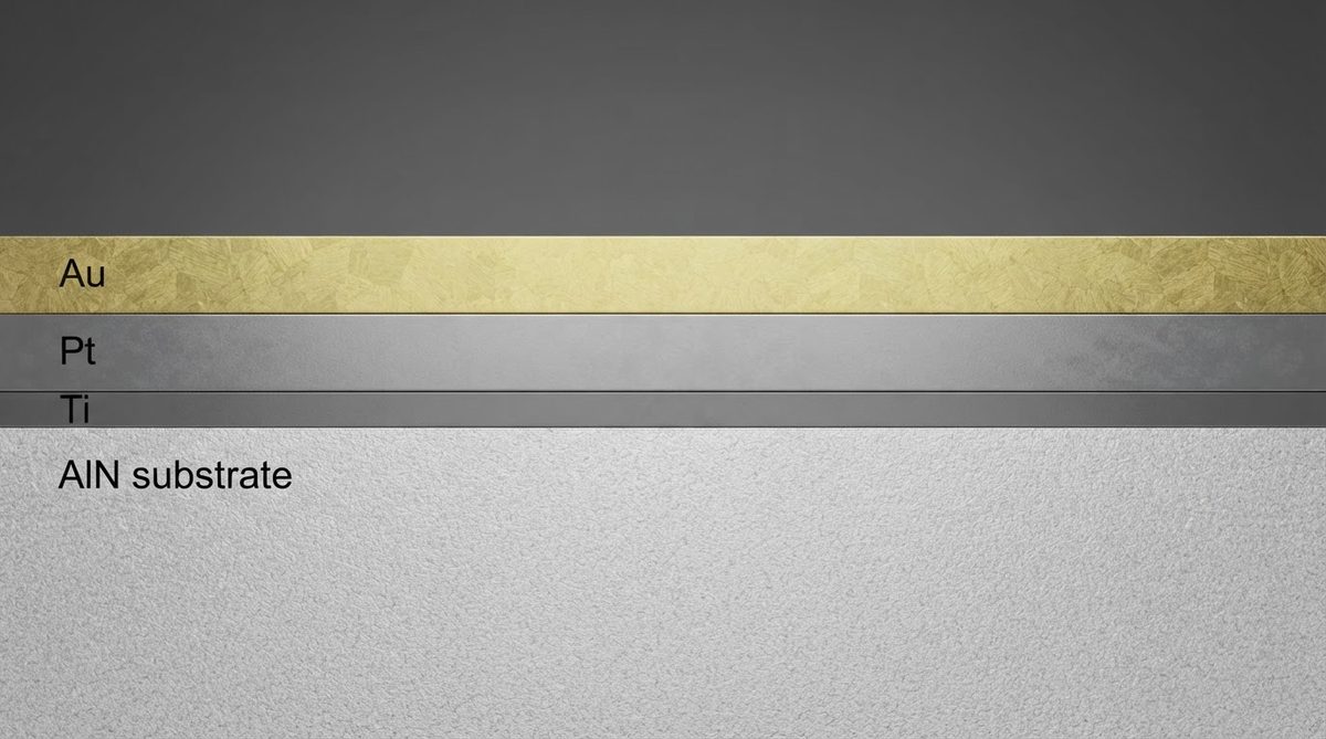
Thin film metallization refers to metal layers deposited under vacuum—typically by DC/RF magnetron sputtering or electron-beam evaporation—onto a polished ceramic surface. Layer thicknesses range from tens of nanometers to a few micrometers. Patterns are defined by photolithography and wet or dry etching, the same process family used in semiconductor wafer fabrication.
This contrasts with thick-film ceramic manufacturing processes, where metal pastes (tungsten, silver, or gold) are screen-printed and fired at 850–1600 °C. Thick film is cheaper and handles higher current, but line/space resolution is limited to roughly 100 µm. Thin film wins whenever feature density, impedance tolerance, or resistor precision matters more than raw conductor thickness.
Aluminum Nitride AlN Thin Film Ceramic Property Comparison
| Parameter | AlN Thin Film Substrate | Al₂O₃ 99.6% Thin Film | Unit | Condition | Source |
|---|---|---|---|---|---|
| Thermal conductivity | 170–230 | 28–35 | W/mK | 25 °C | Maruwa, CoorsTek datasheets |
| Dielectric constant (εr) | 8.5–9.0 | 9.8–10.0 | — | 1 MHz | Kyocera technical catalog |
| CTE | 4.5–4.7 | 7.1–7.4 | ppm/°C | 20–300 °C | CoorsTek ADS-996, Maruwa HA series |
| Surface roughness (Ra) | ≤0.05 (lapped/polished) | ≤0.05 (lapped/polished) | µm | — | Typical vendor spec |
| Dielectric strength | 15–17 | 10–15 | kV/mm | 25 °C, DC | CeramTec Alunit |
| Typical min trace/space | 5–25 | 5–25 | µm | Photolithographic process | Industry standard |
| Max metallization thickness | 0.1–3 | 0.1–3 | µm | Single sputter run | Industry standard |
Typical values for commercially available material, for comparison only. Confirm against the datasheet for your specific grade.
Why Choose AlN Over Alumina for Thin Film Ceramic Circuits?
Both AlN and 99.6% alumina can be lapped to the sub-50 nm Ra surface finish that thin film adhesion demands. The deciding factor is almost always thermal performance. AlN’s thermal conductivity of 170–230 W/mK is 5–8× higher than alumina’s 28–35 W/mK. For a laser diode submount dissipating 5 W through a 0.25 mm substrate with a 2 mm × 2 mm footprint, the steady-state thermal resistance through the substrate alone drops from roughly 1.8 °C/W on alumina to about 0.28 °C/W on AlN—a junction temperature difference that can shift laser wavelength by several nanometers.
AlN’s CTE of 4.5–4.7 ppm/°C also closely matches GaN (3.2 ppm/°C) and SiC (4.0 ppm/°C), reducing solder joint stress in die-attach. For GaAs (5.7 ppm/°C) or Si (2.6 ppm/°C) devices, the mismatch is still manageable with AuSn or SAC solder at these die sizes. If CTE matching to silicon is the top priority and thermal conductivity is secondary, consider quartz substrates (0.55 ppm/°C CTE, but only ~1.4 W/mK).
Enter your substrate area, thickness, and dissipated power below to estimate junction temperature rise through an aluminum nitride AlN thin film ceramic submount.
Thin Film Process Steps on AlN Ceramic
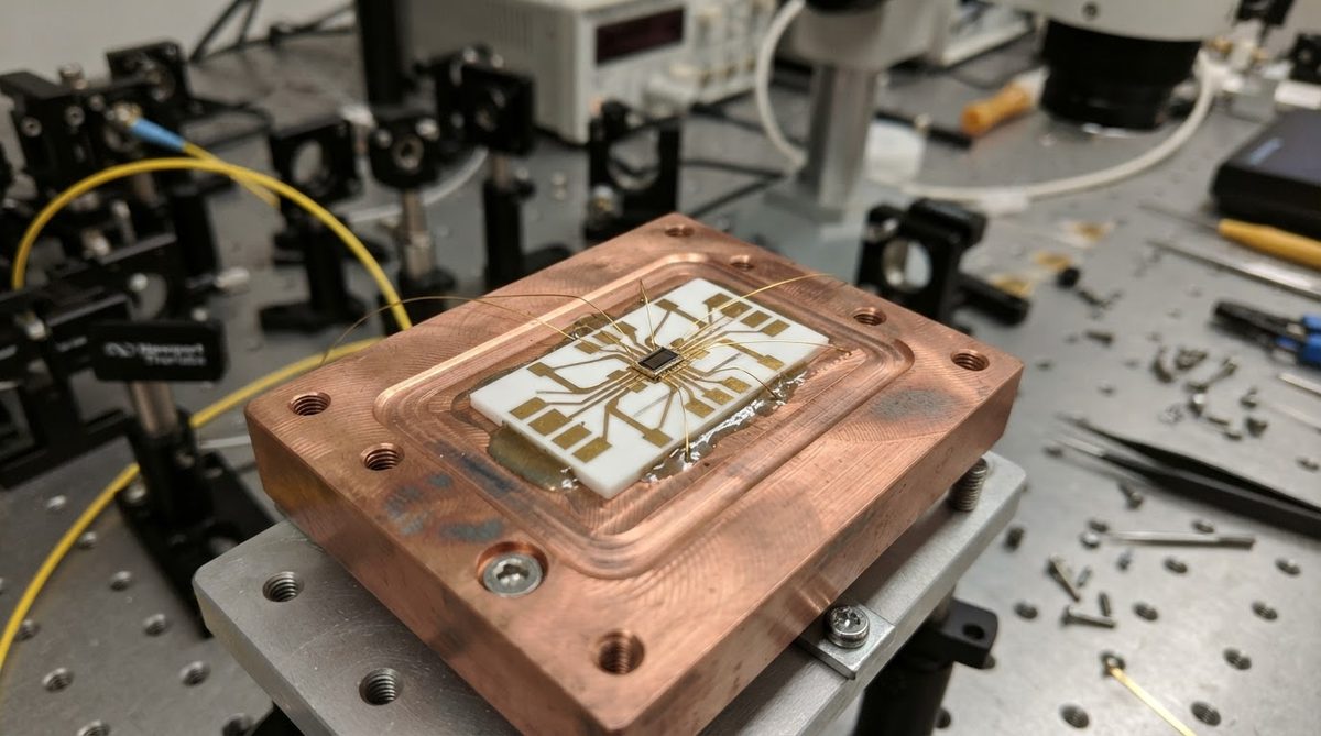
- Substrate preparation. AlN blanks are lapped and polished to Ra ≤ 0.05 µm. Surface contamination is removed with solvent and O₂ plasma cleaning. Any residual oxide layer on AlN is kept thin and uniform.
- Adhesion/barrier layer deposition. A thin Ti or Cr layer (20–100 nm) is sputtered to promote adhesion to the ceramic. A barrier metal—Pt, TiW, or Ni—follows (50–200 nm) to prevent interdiffusion.
- Conductor layer deposition. Au or Cu is sputtered or e-beam evaporated to the target thickness (0.5–3 µm). For thicker conductors, electroplating onto a sputtered seed layer is common.
- Photolithography. Photoresist is spun on, exposed through a mask, and developed. This defines the circuit pattern.
- Etching. Wet chemical or ion-beam etching removes unwanted metal. Lift-off processes are an alternative for some stacks.
- Thin film resistor deposition (optional). TaN or NiCr is sputtered and patterned to form precision resistors with TCR values of ±25–50 ppm/°C, trimmed by laser to ±0.1% tolerance.
- Passivation and singulation. SiN or polyimide passivation is applied where needed. Substrates are laser-scribed or diced. Consult the substrate thickness chart to select the right blank before processing.
Worked Example: Thermal Resistance Through an AlN Thin Film Submount
A GaN HEMT die dissipates 10 W. The aluminum nitride AlN thin film ceramic submount is 0.38 mm thick, and the heat spreads through a 3 mm × 4 mm footprint (12 mm² = 12 × 10⁻⁶ m²). Assume one-dimensional conduction and k = 180 W/mK.
Rth = t / (k × A) = 0.00038 / (180 × 12 × 10⁻⁶) = 0.176 °C/W
Temperature rise through the substrate: ΔT = 10 W × 0.176 °C/W = 1.76 °C. On a 99.6% alumina substrate of the same geometry (k = 30 W/mK), ΔT would be 10.6 °C. That 8.8 °C difference matters for devices where junction temperature directly affects wavelength, gain, or lifetime. For a deeper discussion of thermal stack design, see the AlN thermal design guide.
When Not to Use Aluminum Nitride AlN Thin Film Ceramic
Cost-sensitive, high-volume consumer products. AlN blanks cost 3–5× more than 96% alumina, and thin film processing adds another 2–4× multiplier. If your thermal budget allows alumina, use it.
High-current power circuits needing thick copper. Thin film conductors top out around 3 µm without electroplating. For 100+ µm copper, DBC or AMB on AlN or Si₃N₄ active metal brazed substrates are better suited.
Large panel sizes. AlN substrates are typically available up to about 114 mm × 114 mm (some vendors offer 140 mm × 190 mm). FR-4 or metal-core PCBs serve large-format designs more economically.
Low-frequency, wide-trace designs. If your minimum feature is 150 µm or wider and you do not need integrated thin film resistors, thick-film metallization delivers the same function at lower cost.
Frequently Asked Questions
Can you solder directly to thin film metallization on AlN?
Yes. A standard Ti/Pt/Au or TiW/Ni/Au finish is solderable with AuSn (80/20), SAC305, or indium-based solders. The barrier layer prevents solder leaching into the adhesion layer. Reflow profiles should follow the solder manufacturer’s recommendation; AlN’s thermal mass is low, so ramp rates need control to avoid cracking.
How does thin film AlN handle high temperatures?
Bare AlN ceramic is stable above 1000 °C in inert atmosphere. The practical limit is set by the metallization: Ti/Pt/Au stacks remain reliable to roughly 400–500 °C; TaN resistors are stable to about 300 °C in air. For sustained operation above 500 °C, consult the AlN high-temperature performance data.
What surface finish does AlN need before thin film deposition?
The substrate must be lapped and polished to Ra ≤ 0.05 µm (50 nm). As-fired AlN (Ra 0.3–0.8 µm) is too rough—sputtered films will have poor adhesion and pinholes. Some vendors offer pre-polished blanks ready for deposition.
Is aluminum nitride AlN thin film ceramic suitable for mmWave frequencies above 30 GHz?
AlN works well into the Ka-band and beyond. Its dielectric constant of 8.5–9.0 at 1 MHz is moderate, and loss tangent is typically 0.001–0.003 at 10 GHz (Kyocera data). Thin film’s tight dimensional control keeps impedance variation within ±2–3%, which is critical for transmission lines above 30 GHz.
What is the typical lead time for AlN thin film substrates?
Prototype quantities (5–25 pieces) typically take 4–8 weeks depending on metallization complexity and resistor trimming requirements. Production runs may extend to 8–12 weeks if custom AlN blanks must be sintered and polished first.