Aluminum nitride AlN AMB active metal brazing substrates bond copper foil to AlN ceramic using an AgCu alloy containing a few percent titanium, fired at 780–900 °C in vacuum or inert atmosphere. The result is a metallized ceramic that pairs AlN’s 170–230 W/mK thermal conductivity (per Kyocera and Maruwa datasheets, measured at 25 °C per ASTM E1461) with copper layers thick enough to carry hundreds of amps. This makes aluminum nitride AlN AMB active metal brazing the substrate of choice for high-power IGBT modules, SiC half-bridges, and traction inverters.
What Is Aluminum Nitride AlN AMB Active Metal Brazing?
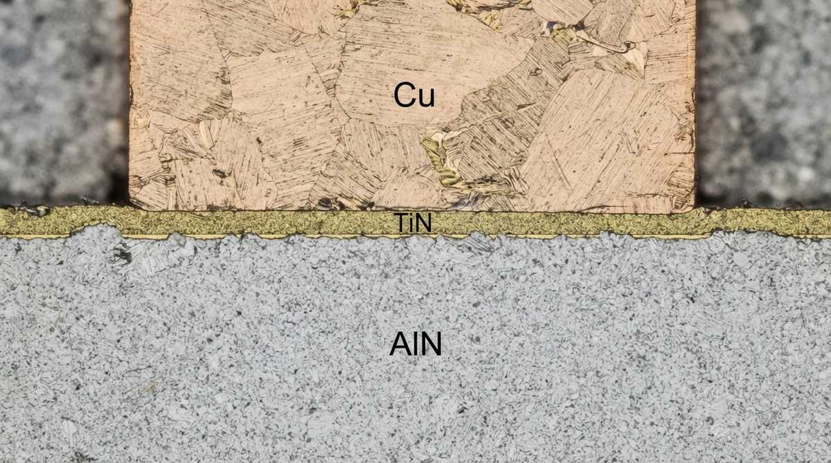
Active metal brazing (AMB) is a vacuum joining process. A braze foil or paste—commonly Ag-Cu-Ti (silver–copper–titanium)—is placed between a copper foil and the AlN ceramic substrate, then heated past the alloy’s liquidus point. The titanium reacts with the AlN surface to form a thin TiN reaction layer, which wets the ceramic and creates a chemical bond rather than a purely mechanical one. After cooling, the copper is patterned by etching.
Because the braze alloy wets the ceramic directly, aluminum nitride AlN AMB active metal brazing achieves higher peel strength (typically 8–15 N/mm per IEC 62047) than oxide-based DBC bonding on AlN. This matters in applications with aggressive thermal cycling: the stronger interface resists delamination longer. For a comparison with oxide-bonded copper on AlN, see AlN DBC ceramic substrates.
Key Properties of AlN AMB Substrates
| Parameter | Value | Unit | Condition | Source |
|---|---|---|---|---|
| Thermal conductivity (AlN) | 170–230 | W/mK | 25 °C, ASTM E1461 | Kyocera / Maruwa datasheets |
| Dielectric strength (AlN) | 15–17 | kV/mm | 25 °C, IEC 60243 | CoorsTek datasheet |
| CTE (AlN) | 4.5–5.0 | ppm/°C | 25–400 °C | CoorsTek / Kyocera |
| Flexural strength (AlN) | 300–400 | MPa | ASTM C1161, 3-pt bend | Maruwa datasheet |
| Copper thickness range | 0.127–0.8 | mm | AMB process | Industry typical |
| Peel strength (Cu–AlN) | 8–15 | N/mm | 90° peel, IEC 62047 | Industry typical |
| Braze alloy | Ag-Cu-Ti | — | ~72Ag-28Cu + 1.5–4% Ti | Wesgo / Morgan |
| Brazing temperature | 780–900 | °C | Vacuum ≤ 10⁻³ Pa | Process standard |
Typical values for commercially available material, for comparison only. Confirm against the datasheet for your specific grade.
Why Choose Aluminum Nitride AlN AMB Active Metal Brazing Over DBC or DPC?
DBC (direct bonded copper) relies on a Cu₂O eutectic to bond copper to ceramic. On Al₂O₃ this works well because alumina provides the oxygen. AlN, however, is a nitride—there is no native oxide layer thick enough for reliable DBC bonding without a pre-oxidation step, and that added oxide layer degrades AlN’s thermal conductivity at the interface. AMB sidesteps this entirely: the Ti in the braze reacts directly with the nitrogen in AlN.
DPC (direct plated copper) deposits copper by sputtering and electroplating, producing very fine traces (down to 20–50 µm line/space) but limited copper thickness—typically ≤ 100 µm. If your design needs thick copper for high current, DPC is not the right fit. You can read more about that approach at AlN DPC ceramic substrates.
AMB gives you both: thick copper (up to 0.8 mm) and a strong, thermally stable bond on AlN. The trade-off is cost and minimum feature size—AMB etching on thick copper rarely achieves traces below 150–200 µm.
Worked Example: Thermal Resistance Through an AlN AMB Stack
Consider a 40 mm × 40 mm AlN AMB substrate, 0.635 mm AlN thickness, 0.3 mm copper on both sides. A SiC die dissipates 200 W over a 10 mm × 10 mm footprint.
One-dimensional thermal resistance through the ceramic alone:
R_th = t / (k × A) = 0.000635 m / (180 W/mK × 0.0016 m²) = 0.0022 °C/W
Adding the copper layers (k_Cu ≈ 390 W/mK, t = 0.3 mm each, same area):
R_th,Cu = 0.0003 / (390 × 0.0016) = 0.00048 °C/W per layer
Total stack R_th ≈ 0.0022 + 2 × 0.00048 ≈ 0.0032 °C/W
At 200 W, the temperature drop across the substrate stack is roughly 0.64 °C. In practice, spreading resistance, solder layers, and the heat-sink interface dominate the total thermal path—but the aluminum nitride AlN AMB active metal brazing stack itself contributes very little.
Enter your substrate dimensions, AlN thickness, copper thickness, and dissipated power below to estimate the thermal resistance of your own AMB stack.
Typical Applications
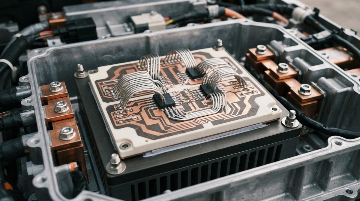
- EV traction inverters — SiC and GaN modules running at junction temperatures above 175 °C need a substrate with low CTE mismatch to silicon carbide (CTE of SiC ≈ 4.0 ppm/°C; AlN ≈ 4.5–5.0 ppm/°C).
- Railway and industrial IGBT modules — thick copper carries bus-bar currents without separate lead frames.
- High-power laser diode sub-mounts — AlN’s thermal conductivity pulls heat from the junction fast enough to prevent wavelength drift.
- RF power amplifiers — GaN-on-SiC transistors benefit from AlN’s combination of thermal performance and low dielectric loss.
When NOT to Use AlN AMB
Aluminum nitride AlN AMB active metal brazing substrates cost roughly 3–5× more than Al₂O₃ DBC at equivalent panel sizes. If your power density is moderate (under ~50 W/cm²) and your thermal cycling requirement is mild (fewer than 2,000 cycles, ΔT < 100 °C), 96% alumina DBC or even an aluminum MCPCB may be sufficient and far cheaper.
If your primary concern is mechanical toughness and extreme thermal cycling (> 3,000 cycles at ΔT > 175 °C), consider silicon nitride AMB ceramic substrates instead. Si₃N₄ has roughly 3× the fracture toughness of AlN (6–8 vs. 2–3 MPa·m^½), which delays crack initiation in the ceramic under cyclic stress—at the expense of lower thermal conductivity (60–90 W/mK).
For fine-pitch circuitry (traces below 100 µm), aluminum nitride thin film ceramic substrates with sputtered metallization are a better match than AMB’s etched thick copper.
AMB vs. DBC on AlN: Side-by-Side
| Parameter | AlN AMB | AlN DBC |
|---|---|---|
| Bonding mechanism | AgCuTi braze, chemical (TiN layer) | Cu₂O eutectic (requires pre-oxidation) |
| Max copper thickness | 0.8 mm | 0.3 mm typical |
| Peel strength | 8–15 N/mm | 4–8 N/mm |
| Min trace/space | ~150–200 µm | ~150–200 µm |
| Thermal cycling reliability | Higher (stronger bond) | Moderate (oxide interface weaker on AlN) |
| Relative cost | Higher | Lower |
Typical values for commercially available material, for comparison only. Confirm against the datasheet for your specific grade.
Design Tips for AlN AMB Layouts
Keep copper pattern symmetry on top and bottom sides to balance residual stress from CTE mismatch between copper and AlN. Asymmetric metallization can cause substrate bow after brazing, especially on thin (0.32 mm) AlN.
Specify edge clearance of at least 0.5 mm from the copper pattern to the substrate edge to prevent electrical arcing and to reduce stress concentration at corners. For available panel and substrate dimensions, check standard ceramic substrate sizes.
Request a dimple or alignment mark on the substrate if you plan automated die attach. AMB vendors can etch fiducials into the copper during patterning at no extra process step.
Frequently Asked Questions
Can AlN AMB substrates handle lead-free soldering?
Yes. The copper surface is typically plated with Ni/Au or NiP/Au, and the substrate easily withstands peak reflow temperatures of 260 °C for SAC305 solder. The braze joint itself was formed at 780–900 °C, so lead-free reflow poses no risk to the bond.
What is the maximum continuous operating temperature for AlN AMB?
AlN ceramic itself is stable above 1,000 °C in inert atmosphere. The practical limit is set by the copper oxidation rate and the braze alloy—continuous use up to 400–500 °C is feasible with appropriate surface protection, though most power module applications operate at junction temperatures below 250 °C.
Does the titanium in the braze affect electrical isolation?
No. The TiN reaction layer is only 1–3 µm thick and is confined to the ceramic–braze interface beneath the copper. The bulk AlN between top and bottom copper patterns provides full dielectric isolation, typically rated at 15–17 kV/mm per IEC 60243.
How does AlN AMB compare to Si₃N₄ AMB on cost?
AlN AMB is roughly 30–50% less expensive than Si₃N₄ AMB for equivalent substrate sizes, primarily because AlN raw material and sintering costs are lower. Si₃N₄ AMB is chosen when thermal cycling life is the dominant requirement, not when cost is the primary driver.
Is wire bonding reliable on AlN AMB copper?
Yes, with the right surface finish. Ni/Au plating supports both aluminum wedge bonding and gold ball bonding. Copper wire bonding directly to bare AMB copper is also practiced in some high-current module designs, though surface roughness from etching should be verified against the wire bonder’s specification.
Next Step
If your power module design needs thick copper on a high-conductivity ceramic, aluminum nitride AlN AMB active metal brazing is the strongest combination of thermal performance and bond reliability available for this class of substrate. To discuss your specific layout, copper thickness, and surface finish requirements, explore AlN thick film substrates for lower-current alternatives, or request a quote for your project.