A 96% alumina LTCC substrate is a multilayer ceramic circuit board made by laminating and co-firing alumina-glass tape at 850–950 °C with silver- or gold-based conductors. The low firing temperature lets designers embed conductors, vias, and passive components inside the ceramic body without melting the metal traces, enabling compact three-dimensional interconnects that post-fired substrates cannot match.
Key Takeaways
- 96% Al₂O₃ LTCC tapes fire at 850–950 °C, roughly half the temperature of HTCC (1 500–1 600 °C), which permits silver and gold conductors instead of refractory tungsten or molybdenum.
- Thermal conductivity of fired 96% alumina LTCC is typically 15–20 W/m·K at 25 °C — lower than dense 96% alumina (24–28 W/m·K) because the glass phase adds porosity.
- Dielectric constant is 9.0–9.5 at 1 MHz (per Kyocera GL550 and CeramTec LTCC tape datasheets), suitable for RF filtering and sensor packaging.
- LTCC supports 10–60+ buried layers, enabling cavity structures, embedded passives, and hermetic packages in a single fired body.
What Is LTCC and How Does the Process Work?
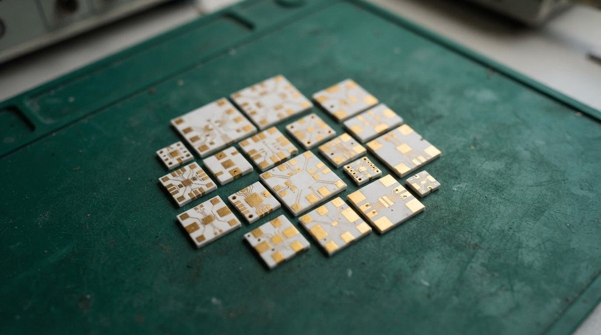
LTCC stands for Low-Temperature Co-fired Ceramic. The process begins with a slurry of alumina powder, glass frit, and organic binders cast into thin green tapes (typically 50–250 µm per layer). Vias are punched or laser-drilled, then filled with conductor paste. Screen-printed traces of silver (Ag), silver-palladium (AgPd), or gold (Au) form the circuit pattern on each layer.
Layers are stacked, aligned, and laminated under heat and pressure (70–80 °C, 20–30 MPa). The laminated block is then co-fired in a single kiln cycle at 850–950 °C. During firing, the glass phase sinters and bonds the alumina grains together while the metal conductors densify simultaneously. The result is a monolithic, hermetic ceramic body with fully embedded wiring.
Because the firing temperature stays below the melting point of silver (961 °C) and gold (1 064 °C), LTCC can use these low-resistivity metals. This is the fundamental advantage over high-temperature co-fired ceramic (HTCC), which fires above 1 500 °C and requires tungsten or moly-manganese conductors with 3–5× higher resistivity.
Material Properties of 96% Alumina LTCC
| Parameter | Value | Unit | Condition | Source |
|---|---|---|---|---|
| Al₂O₃ content | 94–96 | % | After firing | Kyocera GL550 datasheet |
| Firing temperature | 850–950 | °C | Peak, air atmosphere | CeramTec LTCC technical guide |
| Thermal conductivity | 15–20 | W/m·K | 25 °C, ASTM E1461 | Kyocera GL550 |
| Dielectric constant (εr) | 9.0–9.5 | — | 1 MHz, 25 °C | Kyocera GL550 |
| Dielectric loss (tan δ) | 0.001–0.003 | — | 1 MHz, 25 °C | CeramTec LTCC datasheet |
| Flexural strength | 200–320 | MPa | ASTM C1161, 3-pt bend | Kyocera GL550 |
| CTE | 7.0–7.5 | ppm/°C | 25–300 °C | CeramTec |
| Insulation resistance | >10¹⁴ | Ω·cm | 25 °C | Kyocera GL550 |
| X/Y shrinkage tolerance | ±0.1–0.3 | % | Fired vs. design | Industry typical |
Typical values for commercially available material, for comparison only. Confirm against the datasheet for your specific grade.
The glass phase that enables low-temperature sintering also reduces thermal conductivity compared to fully dense 96% alumina. If your design needs 24+ W/m·K, a post-fired 96% alumina thin film substrate is a better thermal path, though it sacrifices the multilayer embedding capability.
LTCC vs. HTCC vs. Post-Fired: Which Process Fits?
| Parameter | 96% Al₂O₃ LTCC | 99.6% Al₂O₃ HTCC | 96% Al₂O₃ Post-Fired (Thin/Thick Film) |
|---|---|---|---|
| Firing temp | 850–950 °C | 1 500–1 600 °C | N/A (substrate pre-fired) |
| Conductor metals | Ag, Au, AgPd | W, Mo, MoMn | Au, Ag, Cu, AgPd |
| Conductor resistivity | Low (Ag ~1.6 µΩ·cm) | High (W ~5.5 µΩ·cm) | Low |
| Layer count | 10–60+ | 10–60+ | 1–2 (surface only) |
| Embedded passives | Yes | Yes | No |
| Thermal conductivity | 15–20 W/m·K | 20–28 W/m·K | 24–28 W/m·K |
| Hermetic cavities | Yes | Yes | No |
| Shrinkage control | ±0.1–0.3% | ±0.3–0.5% | N/A |
Values are representative ranges. Confirm with your substrate supplier for the specific tape system.
Choose LTCC when you need embedded multilayer wiring with low-loss silver conductors, integrated cavities for MEMS or sensors, or RF filter structures where conductor loss matters. Choose HTCC when you need higher thermal conductivity and can tolerate tungsten traces. Choose post-fired thin or thick film when a single- or double-sided layout is sufficient and maximum thermal conductivity is the priority.
Typical Applications
96% alumina LTCC substrates appear most often in RF modules (filters, duplexers, antenna-in-package), automotive radar sensor packages (24 GHz and 77 GHz), MEMS sensor housings, LED driver modules requiring hermetic sealing, and military/aerospace hybrid circuits where MIL-PRF-38534 hermetic packaging is required.
For designs that need silver metallized ceramic on a single layer rather than a full LTCC stack, thick-film silver on a pre-fired alumina blank is simpler and cheaper.
Design Considerations for 96% Alumina LTCC
Shrinkage Management
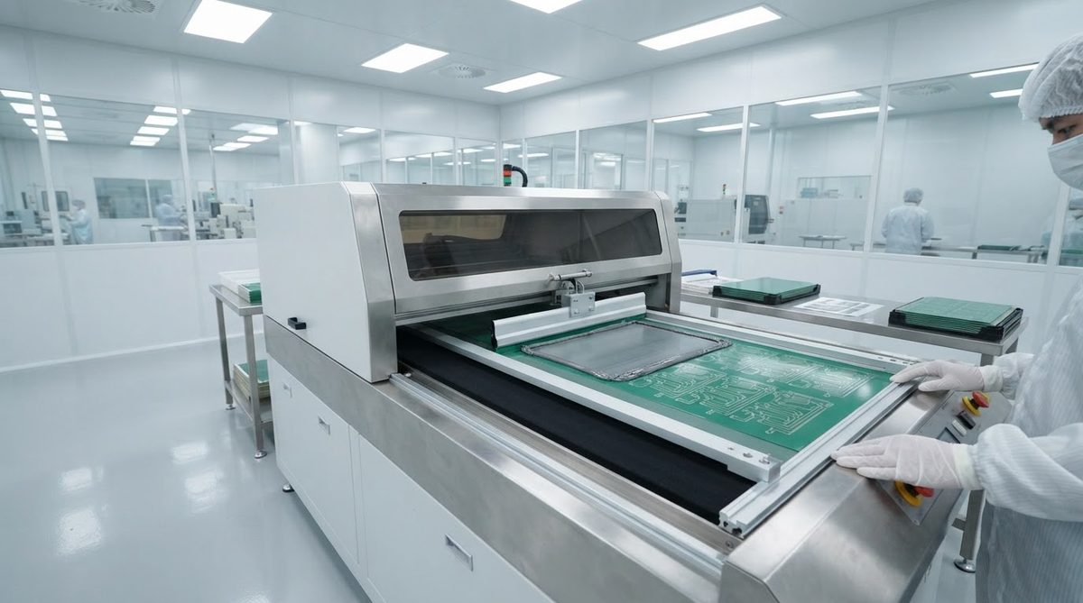
LTCC tapes shrink 12–16% in X, Y, and Z during firing. The exact shrinkage depends on tape composition, lamination pressure, and via density. Zero-shrinkage LTCC techniques (constraining layers that are removed after firing) can hold X/Y shrinkage below 0.1%, but they add process cost. Budget ±0.1–0.3% dimensional tolerance for standard processes and verify with your supplier’s shrinkage data for the specific tape lot.
Via and Line Rules
Minimum via diameter in green tape is typically 75–100 µm after firing. Minimum line width and space for screen-printed Ag conductors is 75–100 µm, though laser-patterned LTCC can reach 25–50 µm. Keep via pitch ≥2× via diameter to avoid delamination at the via barrel.
Layer Thickness Selection
Individual tape layers range from 50 µm to 250 µm (green state). Thinner tapes allow tighter vertical integration but increase layer count and lamination risk. Refer to a ceramic substrate thickness chart for standard fired thicknesses and tolerances.
When Not to Use 96% Alumina LTCC
LTCC is the wrong choice in several common scenarios. If your design is single-sided or double-sided with no embedded passives, a post-fired alumina substrate with thin-film or thick-film metallization is cheaper and offers better thermal conductivity. If you need thermal conductivity above 25 W/m·K through the substrate, LTCC’s glass phase is a bottleneck; consider AlN substrates such as aluminum nitride thin film instead. If your volume exceeds hundreds of thousands of units and the design is simple, organic laminates (FR-4, polyimide, Rogers high-frequency laminates) will cost a fraction per board. Finally, if your operating environment subjects the board to repeated mechanical shock or point-load impacts, ceramic’s brittleness is a liability that no amount of thermal performance can offset.
Frequently Asked Questions
Can you solder standard SMD components onto an LTCC substrate?
Yes. After co-firing, surface pads are typically silver or gold. Standard lead-free solder (SAC305) wets well to both. Use a reflow profile that respects the ceramic’s low thermal mass — ramp rates above 3 °C/s can cause thermal shock cracking in substrates thinner than 0.5 mm.
Does 96% alumina LTCC meet MIL-PRF-38534 hermeticity requirements?
It can. A properly fired and sealed LTCC package routinely passes fine- and gross-leak tests per MIL-STD-883, Method 1014. Hermeticity depends on via fill quality, seam-seal integrity, and the absence of delamination between layers.
How does LTCC dielectric loss compare to Rogers RO4003C at 10 GHz?
96% alumina LTCC has a tan δ of roughly 0.001–0.003 at 1 MHz, rising to 0.002–0.005 at 10 GHz depending on glass composition. Rogers RO4003C specifies tan δ of 0.0027 at 10 GHz. LTCC is competitive on loss but has a much higher εr (9.0–9.5 vs. 3.38), which shrinks wavelength and affects line impedance.
What is the maximum number of layers in a single LTCC stack?
Production LTCC modules with 40–60 layers exist in volume (e.g., Murata and TDK multilayer RF modules). Beyond 60 layers, alignment tolerance and co-planarity become difficult to hold, and most designs restructure into fewer, thicker layers or multiple stacked sub-modules.
Is 96% alumina LTCC suitable for high-power thermal management?
Only marginally. At 15–20 W/m·K, LTCC conducts heat about 30–40% less effectively than dense 96% alumina and roughly 10× less than aluminum nitride. For power modules dissipating more than a few watts per cm², a DBC or AMB substrate on AlN or Si₃N₄ is a better thermal path.
Next Step
If you are evaluating 96% alumina LTCC for a multilayer or hermetic package design, request a ceramic substrate sample kit to verify surface finish and dimensional tolerance against your assembly process before committing to production tooling.