Laser cut alumina parts can be produced to ±25–50 µm positional tolerance on substrates from 0.25 mm to 2.0 mm thick, with no hard tooling and lead times measured in days rather than weeks. CO₂ lasers (9.4–10.6 µm) and UV lasers (355 nm) are the two primary sources used, each suited to different thickness ranges and edge-quality requirements.
Key Takeaways
- CO₂ lasers cut 96% alumina up to roughly 1.5–2.0 mm thick; UV (Nd:YAG 355 nm) lasers are preferred for substrates ≤0.63 mm where minimal heat-affected zone (HAZ) matters.
- Typical positional accuracy is ±25–50 µm; kerf width ranges from 30 µm (UV) to 150–250 µm (CO₂), depending on beam focus and substrate thickness.
- Laser cutting leaves a recast layer 5–30 µm deep on the cut edge; this layer has lower mechanical strength than the bulk ceramic and may need post-processing for high-reliability applications.
- For volumes above roughly 5,000–10,000 pieces, mechanical scribe-and-break or diamond-saw singulation often beats laser on per-part cost.
- 99.6% alumina absorbs the CO₂ wavelength slightly differently than 96% alumina due to its lower glassy-phase content, requiring adjusted power and feed-rate parameters.
How Laser Cutting Works on Alumina
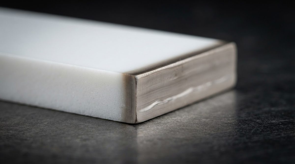
Alumina is transparent in the visible spectrum but absorbs strongly in the mid-infrared (CO₂, 10.6 µm) and is ablated efficiently by UV photons (355 nm). A focused beam heats a narrow line of ceramic above its decomposition point (~2,050 °C for Al₂O₃), vaporising and ejecting material. An assist gas—typically nitrogen or compressed air—blows molten residue out of the kerf.
CO₂ lasers deliver high average power (50–500 W for ceramic work) and cut through thicker substrates quickly. The trade-off is a wider kerf and a more pronounced HAZ. UV lasers operate at much lower average power (3–20 W typical) but remove material through photo-ablation with minimal thermal damage. The choice depends on your substrate thickness, required edge quality, and feature size.
Laser Types Compared for Alumina Cutting
| Parameter | CO₂ (10.6 µm) | UV Nd:YAG (355 nm) | Unit | Notes |
|---|---|---|---|---|
| Typical power range | 50–500 | 3–20 | W | Average power for ceramic substrates |
| Max practical Al₂O₃ thickness | 1.5–2.0 | 0.5–0.63 | mm | Single-pass or multi-pass |
| Kerf width | 150–250 | 30–80 | µm | Depends on focus optics |
| Heat-affected zone depth | 15–30 | 5–10 | µm | Measured by micro-hardness change |
| Positional accuracy | ±30–50 | ±25–35 | µm | Galvo vs. gantry stage dependent |
| Edge roughness (Ra) | 3–8 | 1–3 | µm | As-cut, no post-processing |
| Relative cost per cut-metre | Lower | Higher | — | UV consumables and slower speed |
Typical values for commercially available equipment. Confirm against your laser service provider’s process qualification data.
Achievable Tolerances and Edge Quality
Position tolerance of ±25–50 µm is achievable on most galvanometer-scanned or linear-stage systems. The limiting factors are substrate flatness (bow and warp), fixture accuracy, and thermal drift during the cut. For substrates thinner than 0.38 mm, vacuum chucking is essential to prevent vibration-induced wander.
Edge quality matters for two reasons: mechanical strength and metallisation adhesion. The recast layer left by a CO₂ laser is amorphous alumina mixed with micro-cracks. Flexural strength of a laser-cut edge is typically 20–40% lower than a diamond-sawn edge, per data published by CeramTec for their Rubalit grades. If the cut edge will be a mechanical load path or a seal surface, budget for post-cut lapping or laser-parameter optimisation to minimise recast depth.
For 96% alumina thick-film substrates, the glassy binder phase (~4% SiO₂ + CaO/MgO) melts at a lower temperature than the alumina grains, which can cause localised glass migration to the cut edge. This is cosmetic in most cases but can affect wire-bond pull strength if bond pads are placed within 0.3 mm of the edge.
Design Rules for Laser-Cut Alumina Features
Minimum feature sizes
Internal slots and cutouts should be at least 1.5× the substrate thickness wide. A 0.5 mm thick substrate needs slots no narrower than 0.75 mm. Below this ratio, the assist gas cannot clear debris efficiently, and thermal stress concentrates at the slot corners, risking micro-cracks.
Corner radii
Sharp internal corners are stress risers in any brittle material. Specify a minimum internal radius of 0.15 mm (CO₂) or 0.05 mm (UV). The laser beam itself enforces a minimum radius equal to half the kerf width, so you get some radius whether you specify it or not.
Keep-out from metallisation
Allow at least 0.2–0.3 mm between any conductor trace and the laser cut line. The HAZ can alter the dielectric properties of the ceramic in this zone. For DPC substrates with fine copper traces, this margin prevents delamination caused by thermal shock at the cut edge.
Worked example: estimating cut time
Suppose you need 200 rectangular parts, each 25 × 15 mm, from a 0.635 mm thick 96% alumina panel. Perimeter per part: 80 mm. Total cut length: 200 × 80 mm = 16,000 mm. A CO₂ laser cutting 0.635 mm alumina typically achieves 80–150 mm/s feed rate. At 100 mm/s, cut time is 160 seconds—under 3 minutes of beam-on time. Add panel loading, alignment, and pierce delays, and a realistic cycle is 8–12 minutes for the full batch. Compare this to diamond-saw singulation, which requires a dicing program setup of 15–30 minutes plus individual street cuts at 2–5 mm/s.
96% vs. 99.6% Alumina Under the Laser
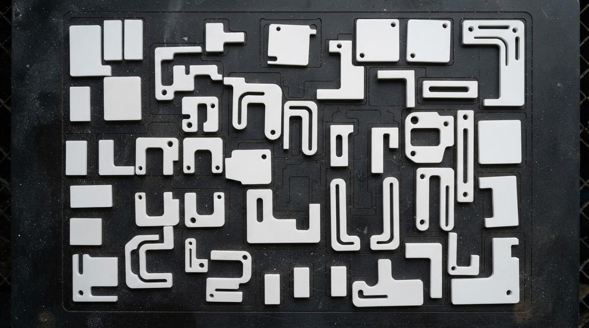
The two grades respond differently. 96% alumina’s glassy phase absorbs CO₂ radiation efficiently and melts first, so the cut propagates partly through melt ejection. 99.6% alumina has almost no glass phase; cutting relies more on direct vaporisation of Al₂O₃ grains, requiring 15–25% more laser power at the same feed rate. Edge roughness on 99.6% substrates is typically 1–2 µm Ra better because there is less resolidified glass.
If your design calls for 99.6% alumina thin-film substrates, confirm that your laser service provider has qualified parameters for this grade specifically. Running 96% parameters on 99.6% material often produces incomplete cuts or excessive chipping on the exit side.
When Not to Use Laser Cutting for Alumina
High volume. Above 5,000–10,000 parts, scribe-and-break using a diamond or carbide wheel is faster and cheaper per piece. The tooling cost amortises quickly, and edge quality is comparable or better.
Thick substrates. For alumina thicker than 2.0 mm, diamond sawing or waterjet-guided laser cutting is more practical. Multi-pass CO₂ cuts on thick stock accumulate thermal damage and taper the kerf.
Tight mechanical tolerances on all surfaces. Laser cutting controls X-Y position well but does not control edge perpendicularity as tightly as diamond grinding. If you need edge squareness better than 2°, plan for a secondary grinding step.
Substrates already metallised on both sides. Cutting through copper layers and ceramic in one pass changes the laser parameters dramatically. Copper reflects CO₂ wavelengths and absorbs UV poorly. Pre-scoring the metal layers or using a two-step process (etch copper streets, then laser ceramic) is standard practice for DBC alumina substrates.
Post-Cut Processing Options
After laser cutting, parts may need one or more finishing steps depending on the application:
- Ultrasonic cleaning in DI water to remove recast debris from the kerf.
- Edge lapping or tumbling to remove the recast layer and restore mechanical strength. This adds 0.5–1 day to lead time.
- Annealing at 900–1,100 °C for 1–2 hours to relieve residual thermal stress in the HAZ. Rarely needed for substrates under 0.635 mm.
- Dimensional inspection using optical CMM or vision systems to verify profile tolerance per ASME Y14.5.
Frequently Asked Questions
Can a standard CO₂ laser cutter (like those used for acrylic) cut alumina?
Generally no. Hobby and signage CO₂ lasers top out at 40–80 W with poor beam quality (M² > 2). Cutting 0.5 mm alumina requires a well-focused beam with M² < 1.5 and at least 50–100 W of power delivered to the substrate. Industrial ceramic laser systems use RF-excited CO₂ sources with superior beam profiles.
Does laser cutting alumina produce hazardous dust?
Yes. Alumina particulate is classified as a nuisance dust, but sub-micron particles generated during laser ablation are a respirable hazard. Proper fume extraction with HEPA filtration is required. The assist gas helps contain the plume, but enclosure ventilation must meet local occupational exposure limits (OSHA PEL for alumina: 15 mg/m³ total dust, 5 mg/m³ respirable fraction).
How does laser cutting affect the dielectric strength of the alumina edge?
The recast layer is amorphous and typically has a lower dielectric strength than bulk polycrystalline alumina. Bulk 96% Al₂O₃ has a dielectric strength of 14–17 kV/mm (per ASTM D149); the recast zone may drop to 8–12 kV/mm. For high-voltage applications, remove the recast layer by lapping or specify a keep-out distance between the conductor and the cut edge.
What file format should I supply for laser-cut alumina parts?
DXF or DWG with dimensions in millimetres is the standard input. Include a separate tolerance callout drawing (PDF) specifying critical dimensions, datum references, and any edge-quality requirements. Gerber files work if the part is being singulated from a metallised panel, but the outline layer must be a closed polyline, not a series of arcs.
Is laser cutting suitable for creating vias or holes in alumina?
UV lasers drill vias down to 50–80 µm diameter in alumina substrates up to 0.38 mm thick. CO₂ lasers produce larger holes (≥150 µm) with more taper. For through-holes in HTCC alumina substrates, punching the green tape before firing is more accurate and cost-effective than post-fire laser drilling.
Next Step
If you have a DXF ready, request a quote to get pricing and lead time for your specific alumina grade, thickness, and quantity. For help choosing between 96% and 99.6% alumina or selecting the right metallisation process, the engineering team at AluminaPCB can review your design files directly.