A custom shape ceramic substrate is a ceramic board profiled to a non-rectangular or non-standard outline, produced by laser cutting, green-state machining, or diamond scribing of the sintered blank. Achievable tolerances range from ±0.025 mm (laser) to ±0.10 mm (green machining), depending on material, thickness, and feature size. The shaping method you choose affects edge quality, cost, and minimum feature geometry, so it pays to understand the trade-offs before you lock your outline drawing.
Key Takeaways
- Laser cutting sintered substrates delivers the tightest tolerances (±0.025–0.05 mm) and cleanest edges, but is slowest per part.
- Green machining (CNC milling or punching before sintering) is the most economical for volume but introduces ~15–20 % linear shrinkage that must be compensated in tooling.
- Minimum slot width is typically 1.5× the substrate thickness for laser-cut parts; narrower slots risk micro-cracking.
- Inside corner radii below 0.2 mm concentrate stress and are a common cause of field fracture in alumina substrates.
- AlN is harder to laser-cut than Al₂O₃ and usually requires a Nd:YAG or UV laser rather than CO₂.
Three Methods for Producing a Custom Shape Ceramic Substrate
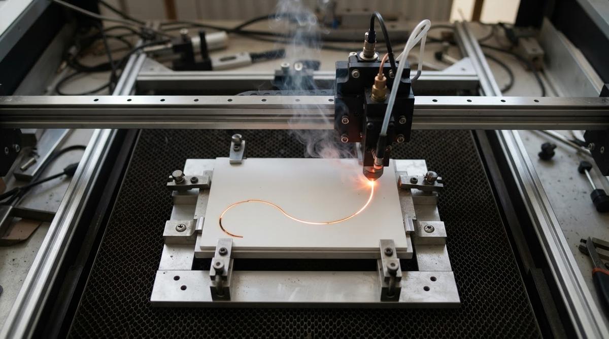
Every custom outline starts with one question: do you shape the ceramic before or after sintering? The answer determines your tolerance budget, edge finish, and unit cost.
1. Laser Cutting (Post-Sinter)
A focused laser beam ablates or thermally fractures the fully sintered substrate along a programmed path. CO₂ lasers (10.6 µm wavelength) work well on alumina. Aluminum nitride absorbs CO₂ poorly, so Nd:YAG (1.064 µm) or UV lasers are used instead. Laser cutting is the go-to method for prototypes and low-to-mid volumes because it requires no hard tooling. Typical positional tolerance is ±0.025–0.05 mm, and kerf width runs 0.05–0.15 mm depending on beam focus and substrate thickness. Edge roughness (Ra) is usually 1–3 µm on 96 % alumina. The main drawback is speed: a complex outline on a 1 mm thick AlN blank can take 30–60 seconds per part, which adds up at 10 k+ volumes. For production quantities of laser-profiled ceramic boards, cycle time is the dominant cost driver.
2. Green Machining (Pre-Sinter)
The ceramic is shaped while still in its “green” (unfired) state, either by CNC milling the pressed or tape-cast blank, or by stamping with a steel die. Green ceramic machines almost like soft chalk, so tool wear is low and throughput is high. The catch is shrinkage: alumina shrinks roughly 15–20 % linearly during sintering (the exact figure depends on powder loading and binder content), and that shrinkage is not perfectly isotropic. You must oversize the green part and accept wider finished tolerances, typically ±0.05–0.10 mm. Stamping with a matched die is fastest for high-volume simple shapes but requires die investment. Green machining is the standard approach for HTCC co-fired ceramic substrates where internal channels or cavities are formed before lamination and firing.
3. Diamond Scribing and Snap (Post-Sinter)
A diamond blade or scribe wheel scores straight lines on the sintered substrate, which is then snapped along the score. This method only produces straight edges and right-angle corners. It is fast and cheap for rectangular singulation but cannot create curves, notches, or interior cutouts. Scribe-and-snap tolerance is ±0.05–0.10 mm, limited by how cleanly the fracture follows the score. If your project requires a true custom shape ceramic substrate with curves or slots, scribing is not an option.
Dimensional Tolerances by Shaping Method
| Parameter | Laser Cut (sintered) | Green Machined | Diamond Scribed |
|---|---|---|---|
| Linear tolerance | ±0.025–0.05 mm | ±0.05–0.10 mm | ±0.05–0.10 mm |
| Minimum inside radius | 0.1 mm (beam limited) | 0.2 mm (tool limited) | N/A (straight only) |
| Minimum slot width | 1.5× thickness | 1.0× thickness | N/A |
| Edge roughness (Ra) | 1–3 µm | 3–6 µm (post-sinter) | 5–15 µm (fracture face) |
| Curves / cutouts | Yes | Yes | No |
| Tooling cost | None (program only) | Low (CNC) to moderate (die) | None |
Typical values for commercially available 96 % alumina, 0.25–1.0 mm thick. Confirm against your supplier’s process capability for your specific grade and geometry.
If your design needs thicknesses outside the common range, review the ceramic substrate thickness chart to confirm what is available as a starting blank before specifying a custom outline.
Geometry Rules That Prevent Cracking
Ceramic is strong in compression but brittle under tension. Every notch, slot, and sharp corner is a stress riser. Following a few geometry rules during layout avoids most field failures on any custom shape ceramic substrate.
Inside corner radii. Specify a minimum 0.2 mm radius on every inside corner. A 90° sharp corner in 96 % alumina concentrates stress by roughly 3–5× compared to a 0.3 mm fillet, per finite-element analyses published by CeramTec (Technical Ceramics design guide, 2022 edition). If your package cavity demands a sharp pocket corner, laser cutting can achieve 0.1 mm radii, but expect a higher scrap rate on substrates thinner than 0.38 mm.
Slot width. Keep slot width ≥ 1.5× substrate thickness for laser-cut parts. A 0.5 mm wide slot in a 0.635 mm thick blank is asking for a micro-crack to propagate from one kerf wall to the other during thermal cycling.
Edge-to-feature clearance. Maintain at least 0.3 mm between the custom outline edge and any metallised trace or via. Laser cutting introduces a heat-affected zone (HAZ) of 0.05–0.15 mm; traces inside the HAZ can delaminate.
Hole placement near edges. Center of any through-hole should be at least 1.5× the hole diameter from the nearest edge. Closer placement risks chipping during handling or reflow.
Enter your substrate dimensions, slot widths, and corner radii below to check whether your custom shape ceramic substrate geometry meets these minimum design rules.
Worked Example: Custom Outline for a Sensor Housing
Suppose you need a 12 mm × 8 mm substrate with a 3 mm diameter center hole and two 1.2 mm wide alignment slots on the long edges, made from 0.635 mm thick 96 % alumina.
- Slot check: 1.2 mm slot width ÷ 0.635 mm thickness = 1.89×. This exceeds the 1.5× minimum. Pass.
- Hole-to-edge check: Hole center is at 6 mm from each short edge and 4 mm from each long edge. Minimum clearance = 1.5 × 3 mm diameter = 4.5 mm. The 4 mm distance to the long edge fails. Fix: shift to a 4.5 mm offset, or reduce hole diameter to 2.5 mm (clearance then needs only 3.75 mm).
- Corner radii: Slot ends need a radius ≥ 0.2 mm. Specify 0.3 mm to give margin.
- Method choice: At 500 pcs, laser cutting is the obvious pick. No tooling cost, ±0.05 mm tolerance on the outline, and the center hole is drilled in the same setup. At 50 k pcs, green-machining with a stamping die would cut unit cost by roughly 40–60 %, but the die itself costs $2 000–$5 000 depending on complexity.
Material Considerations for a Custom Shape Ceramic Substrate
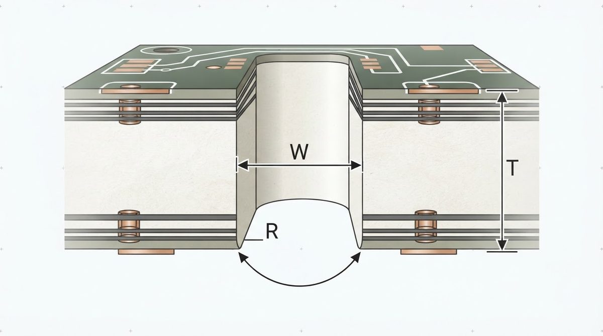
Not every ceramic machines the same way. Alumina (96 % and 99.6 %) is the easiest to laser-cut and the most forgiving of tight radii. Aluminum nitride thin-film substrates require shorter-wavelength lasers and slower feed rates, adding 20–40 % to cutting cost. AlN also has lower fracture toughness (~3 MPa·m^0.5 vs ~3.5–4 MPa·m^0.5 for 96 % alumina, per Kyocera SH-series datasheet), so minimum inside radii should be increased to 0.3 mm.
Silicon nitride (Si₃N₄) is tougher (~6–7 MPa·m^0.5) and more tolerant of aggressive geometries, but it is significantly harder to machine and is typically reserved for power-module substrates where mechanical reliability justifies the cost. Quartz substrates laser-cut cleanly with CO₂ lasers but are limited to applications below ~1 000 °C continuous.
When Not to Use a Custom Shape Ceramic Substrate
If your outline is a simple rectangle that matches a standard ceramic substrate size, skip the custom profiling. You save 15–30 % on substrate cost and avoid the added lead time for laser programming or die fabrication. Standard sizes ship faster and scrap rates are lower.
If your geometry demands wall sections thinner than 0.5 mm over spans longer than 10 mm, ceramic may not survive assembly handling. Consider a metal-core PCB or a machined metal carrier with a bonded ceramic insert instead.
For very high volumes (>500 k/year) of simple shapes, injection-moulded ceramic (CIM) can undercut laser cutting on cost, but CIM requires significant tooling investment and is a separate supply chain.
FAQ
What is the smallest hole you can laser-drill in a ceramic substrate?
Laser-drilled through-holes in sintered alumina go down to about 0.1 mm diameter in substrates up to 0.38 mm thick. Aspect ratios above 3:1 (depth:diameter) risk tapered or incomplete holes. For smaller vias, UV or excimer lasers are used, but cost per hole rises sharply.
Can you add metallisation after custom shaping?
Yes. Laser-cut substrates are routinely metallised with thick-film screen printing or thin-film sputtering after profiling. The key is to cut first, then metallise, so the HAZ does not damage existing traces. If you need metallisation on the cut edge itself (for wraparound grounding, for example), specify it upfront so the process sequence is planned correctly.
Does laser cutting weaken the ceramic?
Laser cutting introduces a heat-affected zone 0.05–0.15 mm deep where micro-cracks can nucleate. Flexural strength of laser-cut 96 % alumina is typically 5–15 % lower than diamond-ground edges, per ASTM C1161 three-point bend tests. For most electronic substrates this reduction is acceptable, but for structural load-bearing parts, post-cut edge grinding restores full strength.
How do I specify a custom shape on my drawing?
Provide a DXF or DWG outline with all dimensions referenced to a single datum. Call out corner radii explicitly, mark toleranced dimensions, and note the material grade and thickness. Include a flat zone or datum edge for orientation during metallisation. Omitting the datum is the most common cause of first-article rejections.
What file formats do ceramic substrate suppliers accept?
Most suppliers accept DXF, DWG, and Gerber (RS-274X) files. For 3D cavity features, STEP or IGES models are preferred. Always include a dimensioned PDF as a cross-check. Vector formats are required; raster images (JPEG, PNG) cannot be used for CNC or laser programming.
Next Step
If you have an outline ready, download the relevant material properties from the ceramic substrate datasheet library to confirm your grade selection, then submit your DXF for a quote. For projects still in the concept stage, requesting a sample kit lets you test fit and handling before committing to a custom run.