Thin film ceramic PCBs use vacuum-deposited metal layers—typically 0.1 µm to 5 µm of copper—on polished ceramic substrates, achieving trace/space geometries as fine as 10 µm. This makes thin film the process of choice for RF/microwave circuits, precision resistor networks, MEMS packaging, and any application where line-width accuracy below 25 µm matters.
Key Takeaways
- Sputtered seed layers range from 0.1 µm to 0.5 µm; electroplated copper builds total thickness to 1–5 µm.
- Minimum trace/space of 10/10 µm is production-proven on 99.6% alumina substrates with Ra ≤ 0.05 µm surface finish.
- Thickness tolerance is typically ±0.2 µm for sputtered layers and ±10% for plated copper.
- Thin film requires a polished substrate surface (Ra ≤ 0.1 µm); rough or as-fired ceramics cause adhesion failures and line-edge defects.
- For copper thicknesses above 10 µm or trace widths above 75 µm, thick-film ceramic processes are usually more cost-effective.
How Thin Film Copper Is Deposited on Ceramic
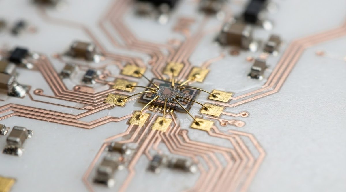
The thin film process begins with a polished ceramic substrate loaded into a vacuum chamber. A titanium or chromium adhesion layer (10–50 nm) is sputtered first, followed by a copper seed layer of 0.1–0.5 µm. This seed provides the electrical path for subsequent electroplating, which builds the copper to its target thickness of 1–5 µm.
Photolithography defines the circuit pattern. A photoresist is spun onto the metallized surface, exposed through a mask, and developed. Copper is then plated into the open areas or, alternatively, the full-sheet metal is etched away from masked regions (subtractive process). Both approaches achieve line-edge roughness below 2 µm on well-polished substrates.
After patterning, the adhesion layer in field areas is removed by a short wet or dry etch. The result is a copper trace that sits on a thin Ti or Cr bonding film, directly on the ceramic. For full thin film layout guidelines, including pad and clearance recommendations, see our dedicated layout page.
Thin Film Copper Thickness Ranges and Tolerances
| Layer | Typical Thickness | Tolerance | Deposition Method |
|---|---|---|---|
| Adhesion (Ti or Cr) | 10–50 nm | ±5 nm | DC magnetron sputtering |
| Seed copper | 0.1–0.5 µm | ±0.05 µm | DC magnetron sputtering |
| Plated copper | 1–5 µm | ±10% | Electrolytic plating |
| Optional nickel barrier | 1–3 µm | ±0.3 µm | Electrolytic or electroless plating |
| Gold finish | 0.05–1.0 µm | ±0.02 µm | Electroless or electrolytic |
Typical values for commercially available thin film processes. Confirm against the datasheet for your specific grade and vendor.
The tight thickness control of sputtering is what makes thin film suitable for precision thin-film resistors (TaN, NiCr) and controlled-impedance RF lines. A ±0.05 µm tolerance on the seed layer translates directly into repeatable sheet resistance values, batch to batch.
Substrate Requirements for Thin Film
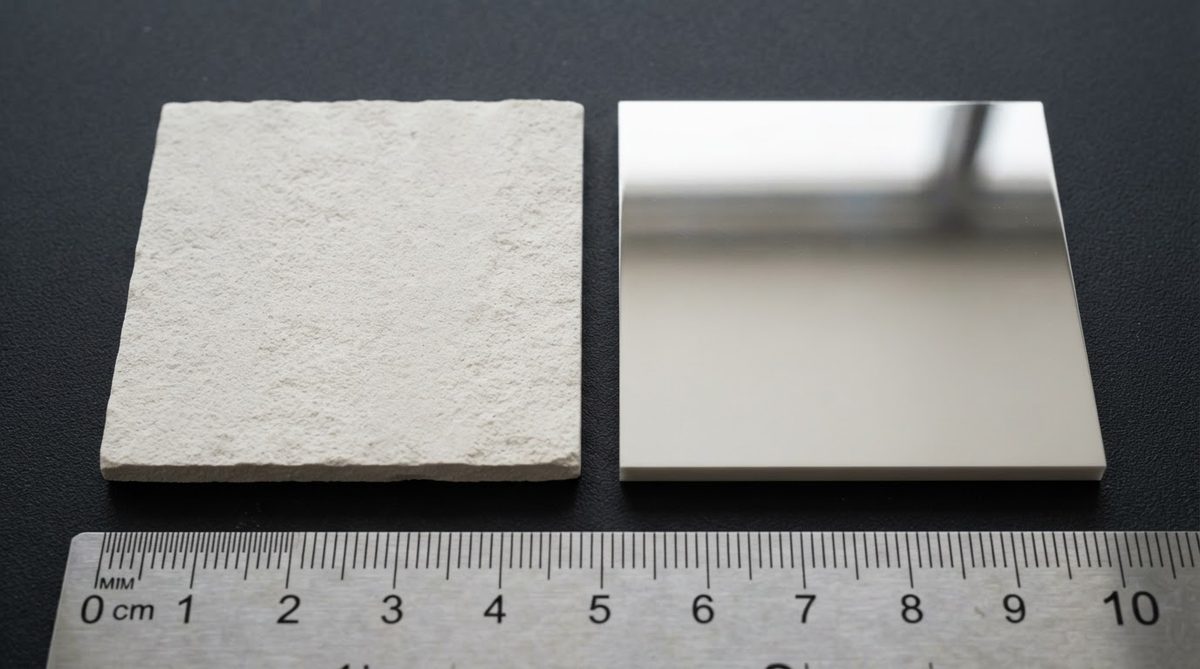
Thin film metallization demands a substrate surface roughness of Ra ≤ 0.1 µm, and ideally ≤ 0.05 µm for traces below 25 µm. Standard as-fired 96% alumina (Ra 0.3–0.8 µm) is too rough; it must be lapped and polished first, or you must specify a pre-polished grade.
The three most common thin film ceramic substrates are:
- 96% alumina (Al₂O₃) — 24–28 W/mK thermal conductivity (per CoorsTek ADS-96R datasheet, 25 °C). Lowest cost. Suitable for most precision analog and sensor circuits.
- 99.6% alumina — 28–35 W/mK. Finer grain structure yields lower Ra after polishing, enabling the tightest trace geometries. Preferred for microwave hybrids and thin-film resistor networks.
- Aluminum nitride (AlN) — 170–200 W/mK (Maruwa AN-200 datasheet, 25 °C). Used when the circuit must also serve as a heat spreader, such as in laser diode submounts or GaN power amplifier carriers.
Substrate thickness for thin film work typically ranges from 0.25 mm to 1.0 mm. Thinner substrates reduce thermal resistance but are more fragile during handling. Consult the ceramic substrate thickness chart for available standard sizes.
Achievable Trace and Space Geometries
| Parameter | Thin Film (Sputtered + Plated) | Thick Film (Screen-Printed) | DBC (Direct Bond Copper) |
|---|---|---|---|
| Min trace width | 10 µm | 75–100 µm | 150–200 µm |
| Min space | 10 µm | 75–100 µm | 150–200 µm |
| Copper thickness | 0.1–5 µm | 8–25 µm (fired) | 127–500 µm |
| Line-edge roughness | < 2 µm | 10–25 µm | 20–50 µm |
| Positional accuracy | ±5 µm | ±25 µm | ±50 µm |
Values represent typical production capability across the industry. Confirm against your vendor’s specification.
For a detailed comparison of minimum features and design constraints, review the design rules for thin film ceramic circuits.
Worked Example: Impedance-Controlled Microstrip on 99.6% Alumina
A 10 GHz microstrip line on 0.254 mm (10 mil) 99.6% alumina (εr ≈ 9.9) requires a trace width of approximately 0.24 mm (240 µm) for a 50 Ω characteristic impedance. With thin film copper at 3 µm thickness, the conductor loss at 10 GHz is roughly 0.08 dB/mm (calculated per the Wheeler incremental inductance rule, assuming conductivity of 5.0 × 10⁷ S/m for plated copper). A thick-film conductor of the same width but with higher surface roughness would add 0.02–0.04 dB/mm additional loss due to the roughness factor. Over a 20 mm feed line, that difference is 0.4–0.8 dB—significant in a low-noise front end.
This example illustrates why thin film is preferred for millimeter-wave and precision RF work: the smooth copper surface on a polished substrate directly reduces insertion loss.
When Not to Use Thin Film Ceramic
Thin film is the wrong process when:
- You need copper thicker than ~5 µm. Power circuits requiring 35 µm or more copper should use DBC or AMB substrates.
- Trace/space is above 75 µm. Thick film screen printing is faster and cheaper for coarser geometries.
- The substrate is unpolished or low-purity. Sputtering onto rough surfaces yields poor adhesion and inconsistent line edges. Budget for polished substrates or switch processes.
- Volume is very high and features are coarse. For millions of simple circuits with features above 100 µm, thick film or LTCC may offer better cost per unit.
- Your budget cannot absorb vacuum processing costs. Thin film requires sputtering equipment, cleanroom photolithography, and polished substrates. Per-unit cost is higher than thick film for equivalent complexity.
Frequently Asked Questions
Can thin film copper carry high current?
Not practically. A 3 µm thick, 200 µm wide copper trace carries roughly 0.3–0.5 A before resistive heating becomes a concern, depending on allowable temperature rise. For currents above 1 A, DBC or thick-film copper with plated build-up is a better fit.
What surface finishes work on thin film ceramic?
Electroless nickel/gold (ENIG), electrolytic gold, and electroless nickel/electroless palladium/immersion gold (ENEPIG) are all compatible. Gold thickness from 0.05 µm (flash) to 1.0 µm (wire-bondable) is standard. Tin-based finishes are rarely used because thin film circuits typically require wire bonding or eutectic die attach rather than solder reflow.
Does thin film ceramic support vias?
Yes. Vias are laser-drilled or mechanically punched in the green-state ceramic before sintering and polishing. They are then filled with conductive paste or plated copper. See via filling capabilities for diameter and aspect-ratio limits.
How does thin film adhesion compare to thick film?
Thin film adhesion relies on the sputtered Ti or Cr layer bonding to the ceramic surface, typically achieving pull strengths of 20–40 MPa (per ASTM F1842 stud-pull test). Thick film conductors, which are sintered into a glass-ceramic matrix, reach 15–30 MPa. Thin film adhesion is adequate for wire bonding and soldering but is more sensitive to substrate surface contamination.
What is the typical lead time for a thin film ceramic prototype?
Industry-wide, expect 3–5 weeks for a first prototype run, including substrate procurement, sputtering, photolithography, plating, and inspection. Complex multilayer thin film builds with embedded resistors may take longer. Confirm lead time at the quoting stage.