Ceramic substrate polishing capability determines how smooth and dimensionally precise a substrate can be made before metallization. Lapping and polishing can bring surface roughness below Ra 0.05 µm and hold thickness tolerance to ±5 µm across a panel. Whether you need that level of finish depends on your metallization method: thin-film sputtering demands it, while thick-film screen printing usually does not.
Why Ceramic Substrate Polishing Capability Matters for Metallization
Every metallization process has a minimum surface-roughness requirement. Sputtered seed layers for thin-film DPC metallization rely on atomic-scale adhesion. Peaks and valleys larger than a few hundred nanometers create shadowed zones where the sputtered metal is thin or absent, leading to opens or weak adhesion after plating. For thin-film ceramic design rules calling for trace widths below 50 µm, surface defects at the substrate level become a dominant yield risk.
Thick-film pastes, by contrast, are 10–15 µm thick after firing and can bridge modest surface irregularities. An as-fired or lapped substrate with Ra 0.3–0.8 µm is usually adequate for thick-film metallized substrates. Polishing that surface further adds cost without improving print quality.
Lapping vs. Polishing: Two Distinct Steps
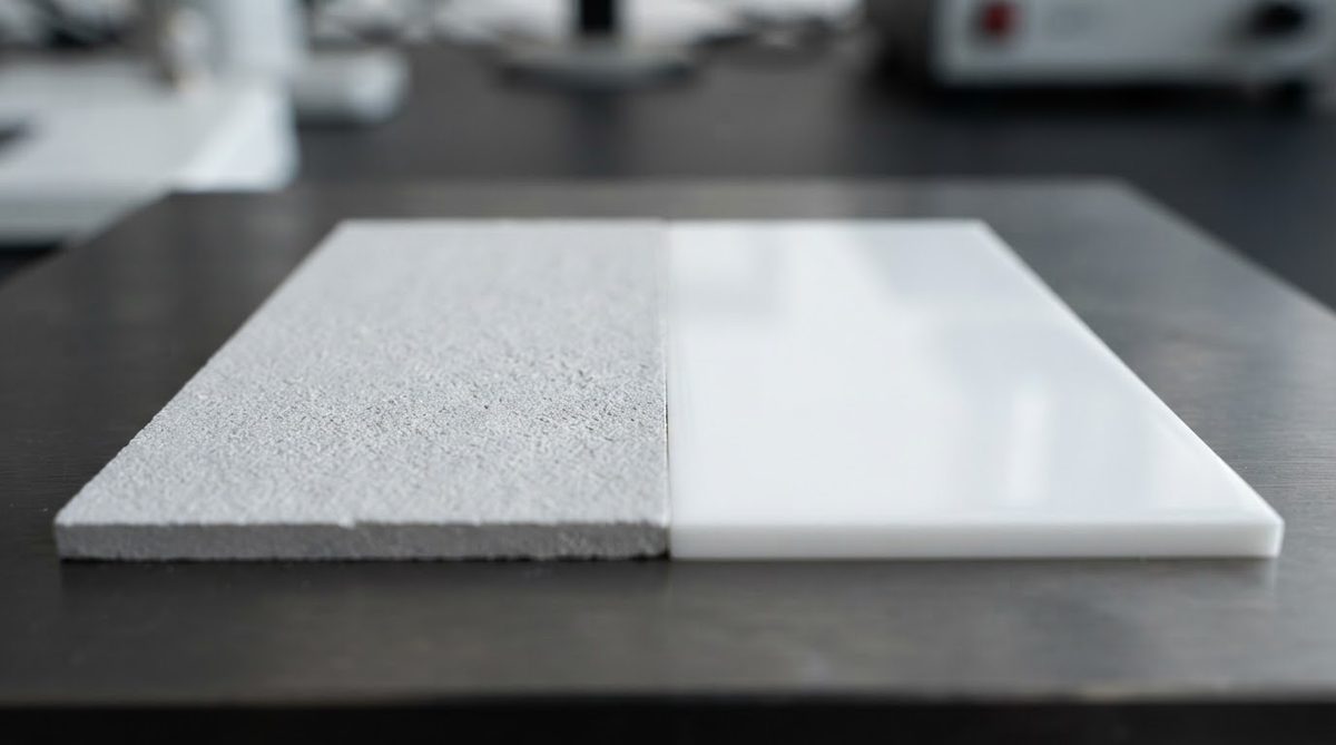
These terms are often used interchangeably, but they are separate operations with different goals, and understanding both is essential to evaluating a vendor’s ceramic substrate polishing capability.
Lapping uses a hard plate and a loose abrasive slurry (typically alumina or silicon carbide grit, 9–25 µm particle size) to flatten the substrate and remove material uniformly. The result is a matte surface with Ra in the 0.1–0.4 µm range and tightly controlled thickness. Lapping is primarily a dimensional operation: it corrects bow, warp, and thickness variation left over from the sintering process.
Polishing follows lapping. It uses progressively finer abrasives—diamond suspensions from 3 µm down to 0.25 µm—on a compliant pad. The goal is to reduce roughness to a mirror or near-mirror finish without removing significant material. Polishing is a surface-quality operation.
A substrate that needs only dimensional correction (flatness, parallelism) can stop after lapping. A substrate destined for thin-film metallization almost always requires both.
Achievable Tolerances by Material
| Parameter | Al₂O₃ 96 % | Al₂O₃ 99.6 % | AlN | Unit | Condition / Note |
|---|---|---|---|---|---|
| Surface roughness (Ra) after lapping | 0.15–0.40 | 0.10–0.30 | 0.10–0.30 | µm | 9 µm Al₂O₃ slurry, measured per ISO 4287 |
| Surface roughness (Ra) after polish | 0.02–0.05 | 0.01–0.03 | 0.02–0.05 | µm | 0.25 µm diamond final stage |
| Thickness tolerance (TTV) | ±10 | ±5 | ±5 | µm | Total thickness variation across 100 mm panel |
| Flatness (bow/warp) | ≤ 25 | ≤ 15 | ≤ 15 | µm | Over 50.8 × 50.8 mm coupon |
| Parallelism | ≤ 10 | ≤ 5 | ≤ 5 | µm | Across substrate |
Typical values for commercially available material, for comparison only. Confirm against the datasheet for your specific grade.
Al₂O₃ 99.6 % polishes to a finer finish than 96 % alumina because its higher purity means fewer glassy-phase inclusions and a more uniform grain structure. AlN achieves similar roughness values but is more sensitive to moisture during polishing; aqueous slurries can cause surface hydrolysis, so many shops use oil-based or semi-aqueous suspensions for aluminum nitride.
Enter your substrate material, target roughness, and thickness to see whether your requirements fall within standard ceramic substrate polishing capability or require special processing.
Worked Example: Specifying a Substrate for Thin-Film DPC
Suppose you are designing a 25 × 25 mm AlN substrate for a GaN power amplifier. The DPC process calls for a Ti/Cu sputtered seed layer at 300 nm total thickness. Your metallization vendor requires Ra ≤ 0.05 µm and TTV ≤ ±10 µm.
- Start with an as-sintered blank. Typical as-sintered AlN has Ra 0.6–1.2 µm and TTV of ±30–50 µm. Neither spec is met.
- Lap to thickness. Using 9 µm SiC slurry, remove 20–40 µm per side to bring TTV within ±5 µm. Surface roughness drops to roughly Ra 0.15 µm. TTV is now met; Ra is not.
- Polish in two stages. First pass with 3 µm diamond brings Ra to ~0.08 µm. Second pass with 0.5 µm diamond reaches Ra 0.03 µm. Both specs are now satisfied.
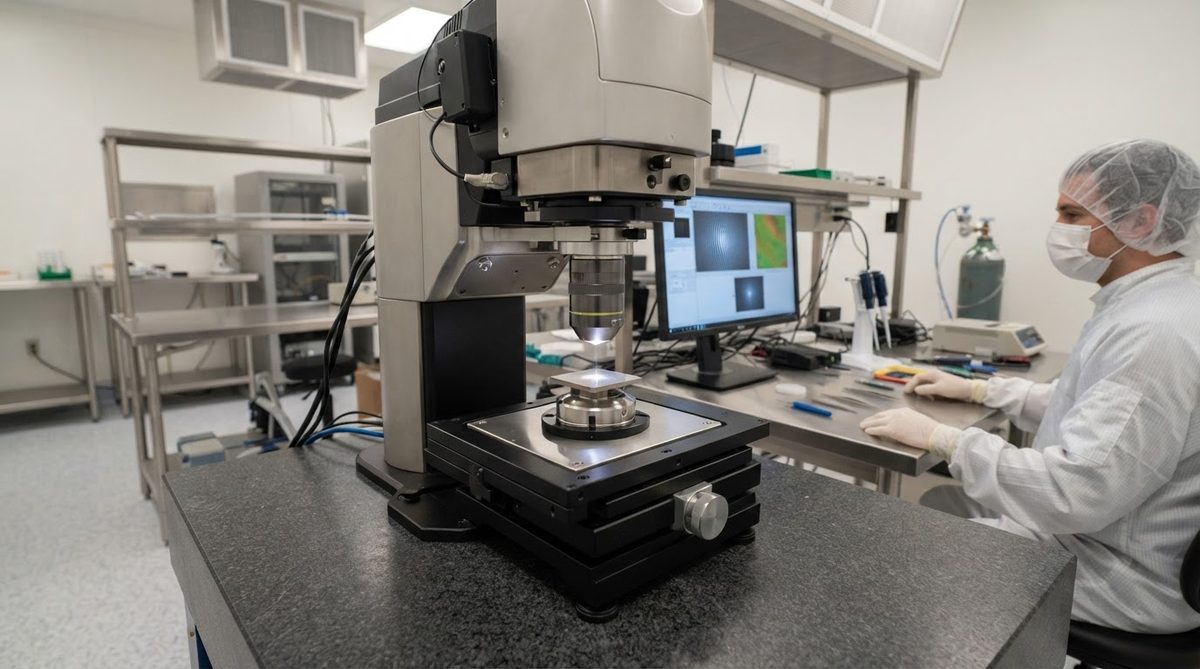
- Clean. Ultrasonic clean in a non-aqueous solvent to remove diamond residue and prevent AlN hydrolysis. Verify Ra with a stylus profilometer or white-light interferometer per ISO 4287.
Total material removal is typically 40–80 µm (both sides combined). Order blanks with enough stock thickness to accommodate this. A 0.635 mm finished substrate should start at 0.70–0.72 mm as-sintered.
Process Factors That Affect Polishing Results
Grain size
Fine-grain ceramics (grain size < 2 µm) polish faster and smoother than coarse-grain material. If your application demands Ra < 0.025 µm, specify a fine-grain grade from your substrate supplier. Standard 96 % alumina with 5–10 µm grains will plateau around Ra 0.04–0.05 µm regardless of polishing time.
Substrate thickness
Thin substrates (≤ 0.25 mm) are fragile under lapping pressure. Breakage rates climb above 5 % for substrates thinner than 0.20 mm unless carrier-mounted. This adds handling cost and should be factored into any assessment of ceramic substrate polishing capability for your project.
Edge quality
Lapping can chip edges, especially on substrates cut by laser scribing and snap separation. If edge quality matters for your assembly, specify edge-rounding or chamfering as a post-polish step.
When Not to Use Polishing
Polishing adds 15–30 % to substrate cost depending on volume and final Ra target. Skip it when:
- Your metallization is thick-film (screen-printed paste). As-fired or lapped substrates with Ra 0.3–0.8 µm work fine.
- The substrate is a thermal spacer or heatsink carrier with no patterned metal. Flatness matters; mirror finish does not.
- Cost is the primary constraint and your trace width is above 100 µm. A lapped-only surface (Ra ~0.2 µm) is often sufficient for DPC at these geometries.
- You are using DBC (direct bonded copper) or AMB (active metal brazing). These processes bond thick copper foil at high temperature; the braze layer fills surface irregularities, so polished substrates offer no adhesion benefit.
FAQ
What surface roughness do I need for sputtering?
Most sputtering processes require Ra ≤ 0.05 µm for reliable seed-layer coverage. Some vendors accept Ra ≤ 0.1 µm for thicker seed layers (≥ 500 nm), but tighter is safer. Confirm with your metallization house before ordering substrates.
Can you polish both sides of a ceramic substrate?
Yes. Double-side lapping and polishing is standard for substrates that carry metallization on both faces or need precise parallelism. TTV targets of ±5 µm are achievable on double-side-processed panels up to 100 mm.
Does polishing weaken the ceramic?
Polishing actually removes surface flaws introduced during sintering and cutting, which can increase flexural strength by 10–20 % compared to an as-fired surface (per ASTM C1161 four-point bend data on 96 % alumina). Subsurface damage from aggressive lapping can offset this gain, so controlled abrasive progression matters.
How do I verify the surface roughness I received?
Request a profilometer report measured per ISO 4287. White-light interferometry (e.g., Zygo or Bruker systems) gives areal roughness (Sa) in addition to line roughness (Ra) and is more informative for polished ceramics. Specify which parameter and cutoff length you require on your drawing.
Is chemical-mechanical polishing (CMP) used on ceramics?
CMP is common for silicon wafers but rarely used for alumina or AlN PCB substrates. The material removal rate on hard ceramics is too low to be cost-effective at PCB-industry volumes. Mechanical polishing with diamond abrasives remains the standard approach.
Next Step
If you are specifying a polished ceramic substrate for thin-film or DPC metallization, read the full guide on ceramic substrate polishing processes for more detail on slurry selection and cleaning protocols. When you are ready to quote, upload your drawing and surface-finish requirements to get a response with pricing and lead time.