DBC direct bonded copper is a process that bonds solid copper foil directly to a ceramic substrate using a copper-oxygen eutectic layer formed at approximately 1065 °C. Standard DBC direct bonded copper thickness ranges from 0.127 mm (5 mil) to 0.8 mm (31.5 mil), with 0.3 mm (12 mil) being the most common grade for power electronics. This thick copper layer gives DBC substrates current-handling ability and thermal spreading performance that thin-film and plated processes cannot match.
What Is DBC Direct Bonded Copper and How Does It Work?
DBC direct bonded copper is a high-temperature bonding method. A sheet of oxygen-free copper (OFC) is placed against a ceramic substrate—typically Al₂O₃ (96% or 99.6%) or AlN—in a controlled-atmosphere furnace. The furnace heats the assembly to just above the Cu–Cu₂O eutectic point (1065 °C). A thin cuprous oxide layer forms at the copper-ceramic interface, wetting the ceramic surface and creating a direct chemical bond upon cooling. No brazing alloy or adhesive is involved.
The resulting bond has high peel strength (typically >4 N/mm per DIN EN 2002-6) and can survive thousands of thermal cycles between −55 °C and +150 °C. Because the copper is a solid sheet rather than a deposited film, it retains bulk copper conductivity (~390 W/mK) and resistivity (~1.7 µΩ·cm at 20 °C).
DBC Direct Bonded Copper Thickness Range and Standard Options
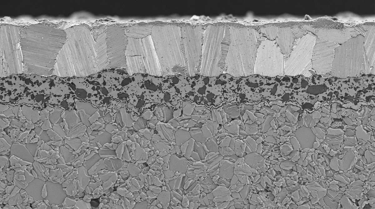
Copper thickness is the primary variable that determines current capacity, thermal spreading, and minimum feature size. Thicker copper carries more current and spreads heat better, but limits how fine you can etch traces.
| Copper Thickness (mm) | Copper Thickness (mil) | Typical Use Case | Min Trace/Space (mm) |
|---|---|---|---|
| 0.127 | 5 | Signal routing, sensor substrates | 0.15–0.20 |
| 0.2 | 8 | Medium-power modules, LED arrays | 0.20–0.30 |
| 0.3 | 12 | IGBT modules, SiC/GaN power stages | 0.30–0.40 |
| 0.5 | 20 | High-current bus bars, EV inverters | 0.50–0.60 |
| 0.8 | 31.5 | Very high current, custom power modules | 0.80–1.00 |
Typical values for commercially available DBC substrates. Min trace/space varies by etch vendor and copper grade. Confirm against your specific supplier’s design rules.
The relationship between copper thickness and minimum trace width is roughly 1:1 to 1:1.5. A 0.3 mm copper layer etches cleanly down to about 0.3–0.4 mm trace/space. Pushing finer than that causes undercut and ragged edges. If your design needs traces below 0.15 mm, consider DPC direct plated copper capabilities instead, which deposits copper by sputtering and plating for much finer resolution.
Substrate Compatibility for DBC Direct Bonded Copper
DBC bonds reliably to three main ceramic materials. Each has different thermal and mechanical trade-offs that affect the finished DBC direct bonded copper substrate’s performance in service.
| Parameter | Al₂O₃ 96% | Al₂O₃ 99.6% | AlN | Unit | Source |
|---|---|---|---|---|---|
| Thermal conductivity | 24–28 | 28–35 | 170–200 | W/mK at 20 °C | CoorsTek, Kyocera datasheets |
| CTE (25–300 °C) | 7.2–7.4 | 7.0–7.2 | 4.5–4.7 | ppm/°C | CoorsTek ADS-996, Kyocera SH-30 |
| Flexural strength | 300–350 | 350–400 | 300–350 | MPa (ASTM C1161) | CeramTec Rubalit |
| Dielectric strength | 12–15 | 14–17 | 14–17 | kV/mm | Kyocera, Maruwa datasheets |
| DBC compatibility | Yes | Yes | Yes | — | — |
Typical values for commercially available material, for comparison only. Confirm against the datasheet for your specific grade.
Si₃N₄ is sometimes bonded with copper, but that process is AMB (Active Metal Brazing), not DBC. The eutectic bonding chemistry of DBC direct bonded copper does not wet Si₃N₄ reliably. If your application demands Si₃N₄ for its superior fracture toughness (>700 MPa), specify AMB instead.
Worked Example: Current Capacity of 0.3 mm DBC Copper
Assume a 10 mm wide, 0.3 mm thick copper trace on an Al₂O₃ DBC substrate. Cross-sectional area = 10 × 0.3 = 3.0 mm². Using bulk copper resistivity of 1.72 µΩ·cm at 20 °C:
Resistance per cm of trace length = ρ × L / A = 1.72 × 10⁻⁶ Ω·cm × 1 cm / 0.03 cm² = 57.3 µΩ/cm.
At 50 A DC, the I²R loss per centimeter = 50² × 57.3 × 10⁻⁶ = 0.143 W/cm. Over a 5 cm trace, that is 0.72 W total. This is manageable for most power module thermal budgets, but the numbers climb fast at higher currents. At 100 A the same trace dissipates 2.87 W over 5 cm, and you need to verify that the substrate can spread that heat without exceeding junction temperature limits.
Enter your trace dimensions, copper thickness, and target current below to estimate resistive losses and temperature rise for your own DBC direct bonded copper layout.
For guidance on pad sizing, isolation gaps, and keepout zones around bonding areas, see the DBC design rules for ceramic PCBs.
DBC vs. Other Ceramic Metallization Methods
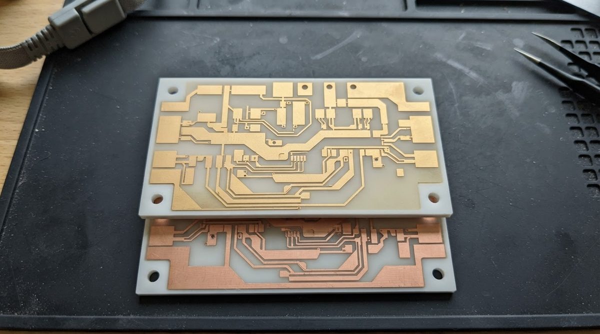
DBC is one of several ways to put copper on ceramic. The right choice depends on your copper thickness requirement and feature resolution.
| Parameter | DBC | DPC | AMB | Thick Film |
|---|---|---|---|---|
| Copper thickness range | 0.127–0.8 mm | 1–200 µm | 0.127–0.8 mm | 10–50 µm (fired) |
| Min trace/space | 0.15–1.0 mm | 30–75 µm | 0.2–1.0 mm | 0.1–0.15 mm |
| Bond mechanism | Cu–Cu₂O eutectic | Sputter + plate | Active braze (AgCuTi) | Glass frit sinter |
| Max operating temp | ~400 °C (limited by Cu oxidation) | ~300 °C | ~400 °C | ~300 °C |
| Best for | Power modules, high current | Fine-line RF, sensors | Si₃N₄ power modules | Resistor networks, hybrids |
Ranges are approximate and vary by supplier. Confirm against vendor specifications.
For a broader view of ceramic metallization capabilities and tolerances, including surface finishes and plating options, see the linked reference.
When NOT to Use DBC
DBC direct bonded copper is not the right process in several common situations:
- Fine-pitch circuits below 0.15 mm trace/space. DBC etching cannot hold these tolerances. Use DPC or thin-film instead.
- Multilayer ceramic circuits. DBC is a surface-bonding process. If you need buried vias, internal routing, or more than two metal layers, HTCC co-fired ceramic or LTCC co-fired ceramic is the correct approach.
- Low-cost, high-volume consumer products. DBC substrates cost significantly more than FR-4 or metal-core PCBs. If your power dissipation is under 5–10 W and junction temperatures stay below 100 °C, an aluminum MCPCB is usually sufficient and far cheaper.
- Si₃N₄ substrates. DBC does not bond reliably to silicon nitride. Specify AMB for Si₃N₄.
Frequently Asked Questions
What is the maximum copper thickness available on DBC substrates?
Standard DBC processes offer copper up to 0.8 mm (31.5 mil). Some specialty suppliers bond copper up to 1.0 mm, but availability is limited and lead times are longer. For most power module designs, 0.3 mm or 0.5 mm copper is sufficient.
Can DBC substrates be used with lead-free solder?
Yes. DBC copper surfaces accept standard Ni/Au, Ni/Ag, or bare copper (OSP) finishes, all of which are compatible with SAC305 and other lead-free solder alloys. The ceramic substrate itself is unaffected by reflow temperatures up to 260 °C.
Does DBC work on both sides of the ceramic?
Yes. Double-sided DBC is standard practice. Copper is bonded to both faces of the ceramic in a single furnace cycle. The bottom copper layer typically serves as a thermal spreader soldered to a baseplate or heatsink.
How many thermal cycles can a DBC substrate survive?
Al₂O₃ DBC substrates typically withstand 3,000–5,000 cycles between −40 °C and +150 °C before delamination or cracking per industry testing (e.g., per IEC 60749-34). AlN DBC tends to have lower cycle life (1,000–3,000 cycles) due to the larger CTE mismatch between AlN (4.6 ppm/°C) and copper (17 ppm/°C). AMB on Si₃N₄ outperforms both in cycling endurance.
What surface finishes are applied to DBC copper?
Common finishes include electroless Ni/Au (ENIG), electrolytic Ni/Au, Ni/Ag, and bare copper with OSP. The finish choice depends on the die-attach method: Au–Sn solder, Ag sintering, or wire bonding each have specific finish requirements.
Next Step
If you are evaluating DBC direct bonded copper for a power module or high-current ceramic circuit, start by reviewing the DBC layout guidelines to confirm your design fits within standard process limits. When you are ready, request a quote with your Gerber files or substrate drawing to get pricing and lead time for your specific copper thickness and substrate material.