DBC direct bonded copper design rules define the minimum trace, space, clearance, and via dimensions you can achieve when laying out a power circuit on a ceramic substrate. DBC substrates support copper layers from 0.127 mm (5 mil) to 0.635 mm (25 mil), bonded to Al₂O₃ or AlN ceramic through a cuprous oxide eutectic process at roughly 1065–1083 °C. The thick copper enables high current carrying capacity, but it also imposes wider minimum trace and space rules than thin-film or DPC processes. Understanding these DBC direct bonded copper design rules before layout prevents costly redesigns.
Key Takeaways
- Minimum trace width for DBC is typically 0.3–0.5 mm, depending on copper thickness—roughly 5–10× wider than DPC or thin-film processes.
- Minimum copper-to-edge clearance should be ≥0.5 mm to prevent delamination at the ceramic border during thermal cycling.
- Al₂O₃ (96%) and AlN are the standard DBC substrates; Si₃N₄ is not processed by DBC but by AMB (active metal brazing).
- Thermal cycling reliability drops sharply when the copper-to-ceramic area ratio exceeds roughly 0.85—leave bare ceramic margins.
- Through-vias in DBC substrates are possible but limited to mechanically punched or laser-drilled holes before bonding, with minimum diameters of 0.3–0.5 mm.
What Is DBC and How Does It Differ from DPC?
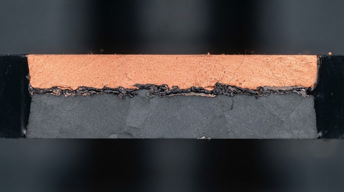
DBC is a process where oxygen-free copper foil is placed on a ceramic substrate and heated in a nitrogen atmosphere containing trace oxygen. At 1065–1072 °C, a thin Cu₂O eutectic layer forms at the copper-ceramic interface, creating a direct metallurgical bond. No adhesive, no seed layer, no plating bath.
This distinguishes DBC from DPC (direct plated copper) design rules, where copper is sputtered as a thin seed layer and then electroplated. DPC achieves finer features (trace/space down to 50 µm or less), but the copper is thinner—typically under 100 µm. DBC starts where DPC stops: thick copper for high-current, high-thermal-dissipation power electronics.
Because the copper is a pre-formed foil rather than a plated deposit, DBC features are defined by chemical etching after bonding. The etch profile through 0.3 mm copper is not vertical—it undercuts significantly, and that undercut sets the practical minimum trace and space.
DBC Direct Bonded Copper Design Rules: Minimum Trace, Space, and Clearance
The table below summarizes typical DBC direct bonded copper design rules for the three most common copper thicknesses. These values represent industry-standard capabilities reported by substrate manufacturers such as Curamik (Rogers) and DOWA.
| Parameter | Cu 0.127 mm (5 mil) | Cu 0.3 mm (12 mil) | Cu 0.635 mm (25 mil) | Unit |
|---|---|---|---|---|
| Min. trace width | 0.20 | 0.30 | 0.50 | mm |
| Min. space (gap) | 0.20 | 0.30 | 0.50 | mm |
| Min. copper-to-edge clearance | 0.40 | 0.50 | 0.75 | mm |
| Etch undercut per side (typical) | ~0.10 | ~0.20 | ~0.40 | mm |
| Dimensional tolerance (etched feature) | ±0.05 | ±0.08 | ±0.12 | mm |
| Surface roughness (Ra, as-bonded) | 0.8–1.5 | 0.8–1.5 | 0.8–1.5 | µm |
Typical values for commercially available DBC substrates, for comparison only. Confirm against the datasheet for your specific grade.
The critical insight: minimum space is governed by etch undercut, not by the lithography mask. A 0.3 mm copper foil etches roughly 0.20 mm laterally per side. If you design a 0.15 mm gap on the mask, the etch will close it entirely. Always add twice the expected undercut to your designed gap. This single rule prevents the most common DBC layout error.
Worked Example: Trace Width for a 50 A Bus Bar
Suppose you need to carry 50 A continuous through a DBC trace on a 0.3 mm copper substrate. The cross-sectional area of a 5 mm wide trace is:
A = 5.0 mm × 0.3 mm = 1.5 mm² = 1.5 × 10⁻⁶ m²
Copper resistivity at 100 °C is approximately 2.0 × 10⁻⁸ Ω·m. For a 20 mm trace length:
R = ρ × L / A = 2.0 × 10⁻⁸ × 0.020 / 1.5 × 10⁻⁶ = 0.267 mΩ
P = I² × R = 50² × 0.000267 = 0.67 W
That 0.67 W is easily managed by the ceramic substrate’s thermal path. But if you narrow the trace to 2 mm to save space, the resistance nearly triples to 0.67 mΩ, and ohmic heating rises to 1.67 W—still modest, but the current density climbs to 83 A/mm², which can cause localized hot spots at solder interfaces. A practical ceiling for DBC traces is 30–60 A/mm² depending on cooling, per Rogers Curamik application guidelines.
Enter your substrate area, thickness, and dissipated power below to estimate junction temperature rise for your own DBC layout.
Substrate Selection for DBC
DBC bonds reliably to two ceramic materials:
- Al₂O₃ 96%: Thermal conductivity 24–28 W/mK at 25 °C (per CoorsTek ADS-96R datasheet). Lower cost, adequate for modules under ~100 W/cm². CTE ~7.2 ppm/°C.
- AlN: Thermal conductivity 170–200 W/mK at 25 °C (per Kyocera SH-30 datasheet). Higher cost, required for high-power IGBTs, SiC MOSFETs, and laser diodes where thermal resistance must be minimized. CTE ~4.5 ppm/°C, closer to silicon (2.6 ppm/°C).
Si₃N₄ is sometimes mentioned alongside DBC, but standard DBC bonding does not work well on Si₃N₄ because the Cu₂O eutectic does not wet silicon nitride surfaces reliably. Si₃N₄ substrates use active metal brazing (AMB) metallization instead, which employs a Ti-containing braze alloy. If your design requires Si₃N₄ for its superior flexural strength (600–800 MPa vs. 300–400 MPa for Al₂O₃ per ASTM C1161), specify AMB, not DBC. Choosing the correct bonding method is one of the most consequential DBC direct bonded copper design rules to get right early.
Copper-to-Ceramic Area Ratio and Reliability
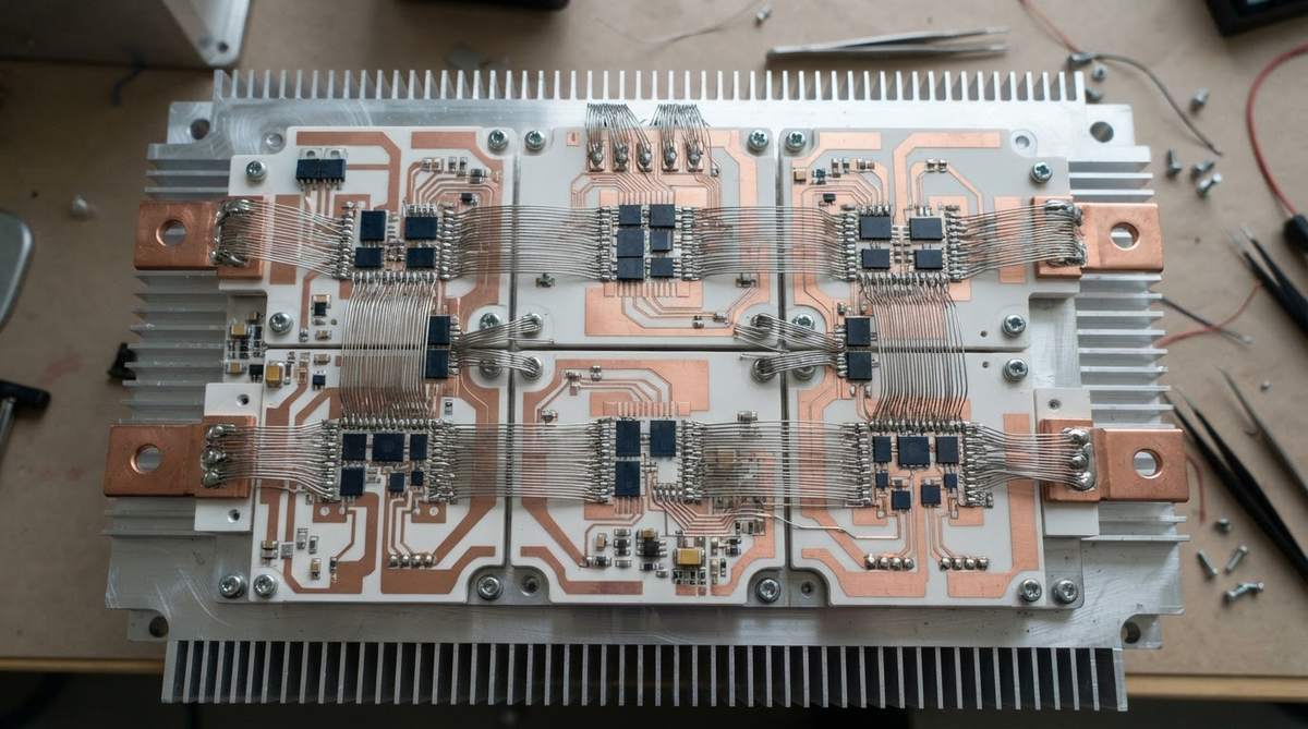
During thermal cycling (e.g., per IEC 60749-34, −40 °C to +150 °C), the CTE mismatch between copper (~17 ppm/°C) and ceramic (~7 ppm/°C for Al₂O₃) generates shear stress at the bond interface. Large unbroken copper planes amplify this stress.
Industry practice limits the copper-to-ceramic area ratio to approximately 0.80–0.85. Above this, crack initiation at the ceramic surface accelerates. Practical countermeasures include leaving a bare ceramic border of ≥0.5 mm around every copper feature, adding stress-relief dimples (small etched holes) in large copper planes, and using thick copper ceramic substrates with matched top and bottom metallization to balance bowing stress.
Via and Through-Hole Constraints
DBC substrates can include through-vias, but the process is constrained. Holes must be punched or laser-drilled in the green or sintered ceramic before copper bonding. Minimum via diameter is typically 0.3–0.5 mm, with an aspect ratio (depth:diameter) limited to roughly 3:1 for reliable copper fill. For substrates requiring dense via arrays or smaller holes, consider DPC processes or LTCC co-fired ceramic design rules, which support vias down to 0.1 mm.
When Not to Use DBC
DBC is the wrong choice when:
- Fine features are needed. If your design requires trace/space below 0.2 mm, use DPC or thin-film. See thin-film ceramic design rules for sub-25 µm features.
- Cost is the primary driver. DBC substrates cost 3–8× more per unit area than FR-4 metal-core PCBs. If your thermal load is under ~20 W/cm² and junction temperature targets are relaxed, an aluminum MCPCB may suffice.
- High-frequency RF circuits. The thick copper and relatively rough surface of DBC increase conductor losses above ~5 GHz. Thin-film on polished alumina or LTCC are better RF choices.
- Complex multilayer routing. DBC is inherently a single-layer or double-sided process. If you need three or more conductor layers with buried vias, LTCC or HTCC is the appropriate technology.
FAQ
Can you solder directly to a DBC substrate?
Yes. DBC copper surfaces accept standard solder alloys (SAC305, SnPb) after appropriate surface finishing such as Ni/Au or Ni/Ag plating. The as-bonded copper surface is often too rough for reliable die attach without a finishing step, so specify a plated finish for die bonding pads.
What is the maximum operating temperature of a DBC substrate?
The Cu₂O bond layer is stable to approximately 400 °C in inert or reducing atmospheres. In air, copper oxidation becomes significant above 250–300 °C. Most power module designs operate with junction temperatures of 150–200 °C, well within DBC limits.
Does DBC work with both sides of the ceramic?
Yes. Double-sided DBC is standard practice. The bottom copper layer typically serves as a thermal spreader and solder interface to a baseplate or heatsink. Balanced copper on both sides also reduces substrate bowing caused by CTE mismatch.
How does DBC compare to AMB for power modules?
DBC uses a Cu₂O eutectic bond and works on Al₂O₃ and AlN. AMB uses a TiAgCu or TiCuSn active braze and works on all three major ceramics including Si₃N₄. AMB achieves higher bond strength (typically 15–25 MPa peel vs. 8–15 MPa for DBC, per Heraeus technical data) and better thermal cycling endurance, but costs more and requires vacuum brazing furnaces.
What surface finishes are available on DBC?
Common finishes include electroless Ni/Au (ENIG), electrolytic Ni/Au, Ni/Ag, and bare copper with an OSP coating. For wire bonding pads, Ni/Au with gold thickness ≥0.5 µm is typical. For large-area soldering, Ni/Ag or Ni/Sn is more cost-effective.
Next Step
If your power module design fits within DBC direct bonded copper design rules for trace and space, the next step is selecting the right substrate material and copper thickness for your thermal budget. Review the heavy copper ceramic PCB options to match copper thickness to your current requirements, then request a quote with your layout files for a design-for-manufacturability check.