Ceramic metallization capability defines what conductor geometries, thicknesses, and adhesion levels you can achieve on a ceramic substrate. The answer depends on the process: thin-film sputtering and plating (DPC) reaches the finest features, thick-film screen printing handles the heaviest deposits, and each method has hard limits that shape your design choices. This page collects the tolerances that matter at layout time.
Key Takeaways
- DPC (thin-film sputtering + electroplating) achieves line/space down to 30/30 µm on 96% Al₂O₃, with copper thickness from 1 µm to roughly 100 µm.
- Thick-film screen printing typically resolves 100/100 µm line/space, with fired conductor thickness of 8–25 µm per print pass.
- Thin-film evaporation or sputtering alone (without plating build-up) produces conductors of 0.1–5 µm, suitable for resistor networks and RF circuits.
- Adhesion strength varies from ~8 N/mm² for thick-film conductors to 15–30 N/mm² for sputtered Ti/Cu seed layers on alumina, measured per ASTM F1842.
- Substrate choice matters: AlN requires a de-oxidation or plasma pre-treatment step before sputtering to achieve reliable adhesion.
Metallization Processes Compared
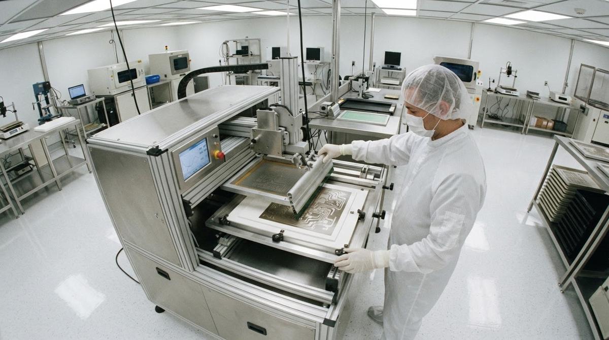
Three processes cover nearly all ceramic PCB metallization. Each trades resolution against thickness capacity and cost.
| Parameter | DPC (Sputter + Plate) | Thick Film (Screen Print) | Thin Film (Sputter/Evap Only) |
|---|---|---|---|
| Min line/space | 30/30 µm | 100/100 µm | 10/10 µm |
| Conductor thickness range | 1–100 µm Cu | 8–25 µm per pass (fired) | 0.1–5 µm |
| Typical conductor material | Cu (Ti/Cu or Cr/Cu seed) | Ag, AgPd, Au, Cu (nitrogen-fired) | Au, Cu, NiCr, TaN |
| Adhesion (peel/pull) | 15–30 N/mm² | 8–15 N/mm² | 15–30 N/mm² |
| Substrate compatibility | Al₂O₃ 96/99.6%, AlN, Si₃N₄ | Al₂O₃ 96/99.6%, AlN (with matched paste) | Al₂O₃ 96/99.6%, AlN, quartz |
| Registration accuracy | ±10–15 µm (photolithographic) | ±25–50 µm (screen alignment) | ±5–10 µm (mask aligner) |
| Cost per dm² (relative) | Medium–High | Low–Medium | High |
Typical values for commercially available processes, for comparison only. Confirm against the datasheet for your specific grade and vendor.
DPC is the workhorse for power-electronics ceramic PCBs because it combines fine features with enough copper to carry current. The process starts with a sputtered Ti/Cu or Cr/Cu seed layer, followed by photoresist patterning and electroplating. After plating, the seed layer outside the pattern is etched away.
Thick-film metallization uses screen printing on ceramic substrates to deposit a paste that is then fired at 850–950 °C in air (for Ag/AgPd) or nitrogen (for Cu). Resolution is limited by the mesh count and emulsion thickness of the screen. Multiple print-and-fire cycles can build conductor thickness, but each pass adds registration error.
Pure thin-film metallization—without a subsequent plating step—targets applications where sub-micron thickness control and very fine features matter more than current-carrying capacity. RF filter networks, precision resistors (NiCr, TaN), and microwave circuits typically use this route. For a deeper look at layout constraints, see the design rules for thin-film ceramic PCBs.
Thickness Capability in Detail
Conductor thickness drives current capacity, thermal spreading, and wirebond reliability. The table below shows practical ranges by process.
| Process | Min Thickness | Max Thickness | Thickness Tolerance | Notes |
|---|---|---|---|---|
| DPC electroplated Cu | 1 µm | ~100 µm | ±5–10% | Uniformity depends on plating bath agitation and pattern density |
| Thick film (single pass, fired) | 8 µm | 25 µm | ±15–20% | Multiple passes can reach 50+ µm total |
| Thin film (sputtered Au) | 0.05 µm | 2 µm | ±5% | Controlled by sputter time and power |
| Thin film (evaporated Au) | 0.1 µm | 5 µm | ±3–5% | E-beam evaporation; lift-off patterning |
Typical values; confirm with your fabricator’s process spec sheet.
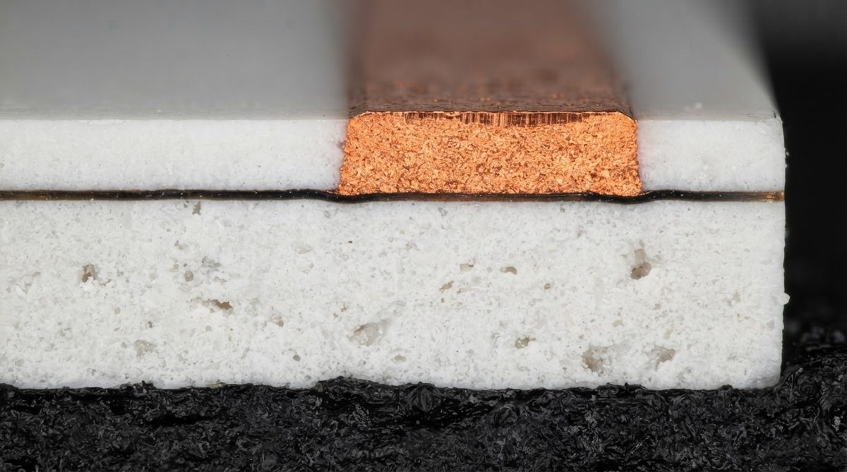
For designs needing copper above 100 µm on ceramic, you move beyond standard DPC into heavy copper capability territory—typically DBC (direct bonded copper) or AMB (active metal brazing), which bond pre-formed copper foil rather than plating it up.
Worked Example: Current Capacity of a DPC Trace
Suppose you need 5 A continuous on a ceramic PCB trace at ΔT ≤ 20 °C above ambient. Using a 50 µm thick, 500 µm wide copper trace on 96% alumina:
- Cross-sectional area: 50 µm × 500 µm = 25,000 µm² = 0.025 mm².
- Per IPC-2152 external-conductor charts (adapted for ceramic’s better thermal spreading), a 0.025 mm² copper cross-section can carry roughly 4–6 A at a 20 °C rise, depending on trace length and surrounding copper density.
- Ceramic’s thermal conductivity (24–28 W/mK for 96% Al₂O₃) spreads heat laterally better than FR-4 (0.3 W/mK), so the effective ΔT is lower than IPC-2152 predicts for the same geometry on organic board.
Result: 5 A is achievable with margin. If you needed 15 A, you would widen the trace or move to a DBC process with 300 µm bonded copper.
Adhesion and Reliability
Metallization adhesion is the single most common failure mode in ceramic PCBs subjected to thermal cycling. Two tests matter:
- Pull test (ASTM F1842 / MIL-STD-883 Method 2011): A 2 mm diameter stud is soldered to the pad and pulled normal to the surface. DPC on alumina typically fails at 15–30 MPa; thick-film Ag on alumina at 8–15 MPa.
- Tape peel test (ASTM D3359): A crosshatch is scribed through the conductor and adhesive tape is pressed on and pulled off. This is a go/no-go screen, not a quantitative measure.
Adhesion on AlN is inherently lower than on alumina because AlN’s native oxide layer is thin and unstable. Plasma cleaning or a reactive Ti adhesion layer (sputtered at 50–100 nm) is essential. Skipping this step can drop pull strength below 5 MPa—enough to survive assembly but not 1,000 thermal cycles from −40 °C to +150 °C.
After metallization, the substrate surface often needs lapping and polishing on the back side or between layers to maintain flatness, especially when thick-film pastes introduce camber during firing.
When Not to Use Ceramic Metallization
Ceramic metallization is the wrong choice when:
- Your design needs >4 layers with fine vias. Multilayer ceramic (LTCC/HTCC) exists but is expensive and limited in via density compared to organic HDI. For >6 layers at 100 µm vias, standard FR-4 or polyimide HDI is cheaper and faster.
- Board area exceeds ~150 mm × 150 mm. Ceramic substrates are brittle and difficult to handle in large panels. Metal-core PCBs (MCPCBs) handle large-format thermal management at lower cost.
- Budget is the primary constraint. Even thick-film ceramic costs 5–15× more per cm² than FR-4. If your thermal and dielectric requirements can be met with an aluminum MCPCB, that is the pragmatic choice.
- You need flex or conformal shapes. Ceramic does not bend. Polyimide flex circuits are the obvious alternative.
Frequently Asked Questions
Can I mix thick-film and thin-film metallization on the same substrate?
Yes. A common hybrid approach uses thick-film conductors for power traces and thin-film resistors (NiCr or TaN) for precision networks, all on one 96% alumina substrate. The thick-film layers are printed and fired first; thin-film is deposited afterward at lower temperature so it does not disturb the fired conductors.
What surface finishes work on ceramic metallization?
ENIG, ENEPIG, immersion Ag, and electroplated Au are all used. ENIG (3–5 µm Ni / 0.05–0.1 µm Au) is the most common for soldering. Wirebondable gold pads typically need 0.5–1.5 µm electroplated Au over Ni. The finish choice depends on your assembly method, not the metallization process.
Does metallization affect the substrate’s dielectric constant?
The metallization itself does not change the bulk dielectric constant of the ceramic (εr ≈ 9.8 for 96% Al₂O₃ at 1 MHz per CoorsTek datasheet). However, conductor geometry and ground-plane proximity determine the effective impedance of a transmission line. Treat it as a standard microstrip or stripline calculation using the ceramic’s εr.
How tight can via registration be with DPC metallization?
DPC photolithography aligns vias to ±10–15 µm relative to the conductor pattern on the same side. Layer-to-layer registration through the substrate depends on the via filling and drilling process and is typically ±25–50 µm for laser-drilled, copper-filled vias in alumina.
Is gold metallization necessary for wirebonding?
For gold ball bonding, yes—you need a gold top surface, typically ≥0.5 µm electrolytic Au. Aluminum wedge bonding can be done on bare thick-film conductors or on nickel-plated pads without gold. The bonding method dictates the finish requirement.
Next Step
If you have a layout in progress, review the ceramic metallization process overview to match your design to the right process family. When you are ready for a quote with specific trace/space and thickness requirements, submit your files for pricing.