LTCC (low-temperature co-fired ceramic) is a multilayer ceramic technology that laminates unfired “green” tape layers with screen-printed conductors and fires the entire stack at 850–900 °C. Internal conductor thickness is typically 10–15 µm per printed layer, while post-fired surface metallization can reach 20–30 µm with additional plating building copper up to roughly 100–300 µm depending on the process. Because firing happens below the melting point of silver and gold, LTCC uses these metals natively, though copper is possible in nitrogen-atmosphere kilns.
Key Takeaways
- LTCC co-fires green ceramic tape and printed conductors at 850–900 °C, well below the ~1600 °C required by HTCC.
- Internal conductor thickness per printed pass is 10–15 µm; multiple prints on a single layer can reach 20–25 µm before lamination.
- Layer counts of 10–60+ are production-proven, enabling complex 3D routing, embedded passives, and cavity structures.
- Minimum via diameter is typically 75–100 µm (laser-punched), with filled vias providing vertical interconnects between every layer.
- Silver and gold are the standard conductor metals; copper co-firing requires an oxygen-free atmosphere and tighter process control.
What Is LTCC Co-fired Ceramic?
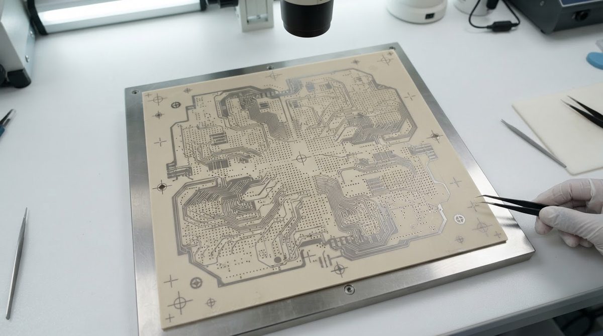
LTCC is a ceramic substrate technology where individual layers of glass-ceramic tape (typically alumina-glass composites with a dielectric constant of 5.5–8.0 at 1 MHz) are blanked, via-punched, screen-printed with conductor paste, stacked, laminated under isostatic pressure, and co-fired in a single kiln cycle. The “low temperature” label refers to a peak firing temperature of 850–900 °C, which is low relative to HTCC’s 1500–1600 °C. This lower temperature is what permits the use of high-conductivity metals like silver (σ ≈ 6.3 × 10⁷ S/m) and gold instead of the refractory tungsten or molybdenum required by HTCC co-fired ceramic.
The green tape itself is a slurry-cast film, typically 50–250 µm thick per layer after firing. Shrinkage during firing is significant: 12–16% in X-Y and 15–25% in Z, per Ferro and DuPont LTCC system datasheets. Designers must account for this shrinkage in every dimension, including via registration and cavity depth. Zero-shrinkage LTCC systems (from Ferro, Heraeus) constrain X-Y shrinkage to under 0.1% by using sacrificial constraining layers, which improves positional accuracy to ±25 µm or better.
Conductor Metals and Thickness Ranges
The table below summarizes achievable conductor thicknesses for the metals commonly used in LTCC. Values assume standard screen printing on green tape before lamination and firing.
| Parameter | Silver (Ag) | Gold (Au) | Copper (Cu) | Unit | Condition |
|---|---|---|---|---|---|
| Internal conductor thickness (single print) | 8–15 | 8–12 | 10–15 | µm | After co-firing |
| Internal conductor thickness (double print) | 18–25 | 15–20 | 18–25 | µm | After co-firing |
| Surface conductor thickness (printed) | 10–20 | 8–15 | 10–20 | µm | Post-fire print + refire |
| Surface conductor thickness (printed + plated) | Up to 50 | Up to 30 | Up to 100–300 | µm | Electroplated after firing |
| Minimum line width | 75–100 | 75–100 | 100–125 | µm | Standard screen, 325–400 mesh |
| Minimum line space | 75–100 | 75–100 | 100–125 | µm | Standard screen |
| Firing atmosphere | Air | Air | N₂ (O₂ < 10 ppm) | — | Peak 850–900 °C |
Typical values for commercially available LTCC systems (DuPont 951/9K7, Ferro A6M/A6S, Heraeus CT2000). Confirm against the datasheet for your specific grade.
Copper co-firing in LTCC demands tight oxygen control throughout the binder burnout and sintering stages. Organic binders in the green tape must be removed before sintering, which normally happens in air. With copper, a two-stage profile is used: slow burnout in a low-oxygen or wet-nitrogen atmosphere, followed by sintering in dry nitrogen. This adds process complexity and cost compared to silver-based LTCC. For designs that need thicker copper on the surface for power handling, post-fire electroplated copper buildup on a thin co-fired seed layer is the standard approach.
Via and Interconnect Capabilities
LTCC vias are punched or laser-drilled in the green tape before printing, then filled with conductor paste and co-fired. This produces solid, filled vias that carry current and conduct heat vertically through the stack. Stacked vias across multiple layers create thermal and electrical columns.
- Minimum via diameter: 75–100 µm (laser-punched); 150–200 µm (mechanical punch).
- Via pitch: Minimum center-to-center is typically 2× the via diameter, so 200 µm pitch for 100 µm vias.
- Via-to-edge clearance: ≥125 µm from the nearest conductor edge to avoid cracking during lamination.
- Thermal vias: Arrays of filled vias under power devices reduce thermal resistance. A 5×5 array of 200 µm silver-filled vias through 0.5 mm of LTCC substrate drops thermal resistance by roughly 40–50% compared to bare ceramic, per Kyocera application data.
Consult the LTCC design rules for minimum keep-out zones, pad-to-via ratios, and layer-specific registration tolerances before committing your layout.
Layer Count and Substrate Dimensions
Production LTCC modules commonly use 10–40 layers. Specialty RF and sensor packages have been demonstrated at 60+ layers. Each fired layer is 50–250 µm thick, so a 20-layer stack with 100 µm layers yields a total substrate thickness of roughly 2 mm after firing (accounting for Z-shrinkage). Maximum panel size before firing depends on the tape manufacturer’s casting width, typically 150 mm × 150 mm for standard production, with some facilities handling 200 mm × 200 mm green sheets. After firing, panels are separated by laser scribing or diamond dicing.
Worked Example: Estimating Internal Conductor Resistance
Suppose you need a 50 mm long, 150 µm wide silver trace on an internal LTCC layer, single-print (12 µm thick after firing). Silver’s bulk resistivity is 1.59 × 10⁻⁸ Ω·m; co-fired silver paste is roughly 1.5–2× bulk, so use 2.8 × 10⁻⁸ Ω·m.
R = ρ × L / (w × t) = 2.8 × 10⁻⁸ × 0.05 / (150 × 10⁻⁶ × 12 × 10⁻⁶) = 0.78 Ω
For a power bus carrying 500 mA, that gives a voltage drop of 0.39 V and 0.19 W of resistive heating. If this is unacceptable, widen the trace to 300 µm (halving resistance to ~0.39 Ω) or use a double-print layer (24 µm, ~0.39 Ω at 150 µm width). This kind of calculation matters early in LTCC layout planning because conductor thickness is fixed at the printing stage, not easily changed later.
LTCC vs. Thick Film and Thin Film: When Each Fits
LTCC is not the only way to metallize a ceramic substrate. The choice depends on layer count, conductor thickness, and feature size.
| Parameter | LTCC | Thick Film | Thin Film |
|---|---|---|---|
| Layer count | 10–60+ | 1–4 (print-and-fire cycles) | 1–3 (sputter + plate) |
| Internal conductors | Yes (co-fired) | No | No |
| Min line/space | 75–125 µm | 100–150 µm | 10–25 µm |
| Conductor thickness | 10–25 µm internal; up to 300 µm plated surface | 10–50 µm printed; up to 300 µm plated | 0.5–5 µm sputtered; up to 100 µm plated |
| Embedded passives | Resistors, capacitors, inductors | Resistors | Resistors, capacitors (thin-film) |
| Typical application | RF modules, sensors, MCMs | Power hybrids, heaters | mmWave, precision analog |
Comparison is for standard production processes. Confirm against your supplier’s specific capability sheet.
For single- or double-sided power circuits where you need 50–300 µm of copper, thick-film printed ceramics or DBC/AMB are simpler and cheaper. LTCC’s strength is vertical integration: burying passive components, routing RF signals through stripline structures, and creating hermetic cavities for MEMS or sensors.
When Not to Use LTCC
LTCC is the wrong choice when your design is single-layer or double-layer with no embedded passives. A thick-film or thin-film metallized alumina substrate will cost less and deliver faster. It is also a poor fit for high-current power electronics above 20–30 A per trace, because co-fired conductor thickness tops out around 25 µm internally. DBC or AMB on alumina or silicon nitride handles that better. If your dielectric constant requirement is below 4.0 (e.g., low-loss RF above 40 GHz), consider PTFE-ceramic laminates or fused silica substrates instead of LTCC’s 5.5–8.0 range. Finally, if your volume is under 50 units and you do not need multilayer, the NRE for LTCC screen sets and lamination tooling is hard to justify.
Frequently Asked Questions
Can you co-fire copper in LTCC?
Yes, but it requires firing in a nitrogen atmosphere with oxygen below 10 ppm. A modified binder burnout profile removes organics without oxidizing the copper. This adds cost and limits the number of qualified paste suppliers compared to silver-based LTCC.
How thick can copper get on an LTCC surface?
The co-fired printed layer is 10–20 µm. After firing, electroplating can build copper up to 100–300 µm on the surface. The practical limit depends on adhesion of the co-fired seed layer and plating uniformity across the panel.
What is the dielectric constant of LTCC tape?
Standard LTCC tapes range from 5.5 to 8.0 at 1 MHz, depending on the glass-ceramic composition. DuPont 951 is approximately 7.8; Ferro A6M is approximately 5.9. Low-K LTCC tapes (εr ≈ 4.0–5.0) exist but are less widely available. Always use the tape manufacturer’s datasheet value at your operating frequency.
How does LTCC shrinkage affect via registration?
Standard LTCC shrinks 12–16% in X-Y during firing, which can cause via misregistration of ±50–75 µm in a 150 mm panel. Zero-shrinkage LTCC systems reduce X-Y shrinkage to under 0.1%, improving registration to ±15–25 µm. If your via pitch is below 300 µm, zero-shrinkage tape is strongly recommended.
Is LTCC hermetic?
Yes. A properly fired LTCC body with brazed or seam-welded lids achieves helium leak rates below 1 × 10⁻⁸ atm·cc/s, meeting MIL-STD-883 Method 1014 for fine-leak hermeticity. This makes LTCC suitable for MEMS packaging, military hybrids, and implantable medical devices.
Next Step
If your design needs multilayer ceramic routing with embedded passives or hermetic cavities, LTCC is likely the right process. Review the alumina 96% LTCC substrate options for material specifications, or request a quote with your layer stackup and conductor requirements to get lead time and pricing for your specific design.