An aluminum nitride AlN thin substrate is a ceramic sheet typically 0.25–0.635 mm thick with thermal conductivity of 170–200 W/mK at 25 °C, making it the highest-conductivity oxide-free ceramic substrate commercially available for PCB and power-module applications. These substrates serve as the base layer for thin-film and thick-film metallization in high-power LEDs, RF amplifiers, and IGBT modules where every fraction of a millimeter in the thermal path matters.
Key Takeaways
- Aluminum nitride AlN thin substrate thicknesses range from 0.25 mm to 0.635 mm, with thermal conductivity of 170–200 W/mK depending on purity and sintering process (per Maruwa and Kyocera datasheets).
- Coefficient of thermal expansion (CTE) is 4.5–4.7 ppm/°C at 20–400 °C, closely matching silicon (3.5 ppm/°C) and SiC (4.0 ppm/°C).
- Dielectric strength exceeds 15 kV/mm (per ASTM D149), supporting high-voltage isolation in thin cross-sections.
- Cost runs 3–5× higher per unit area than 96% alumina substrates of the same dimensions.
What Makes an Aluminum Nitride AlN Thin Substrate Different from Alumina
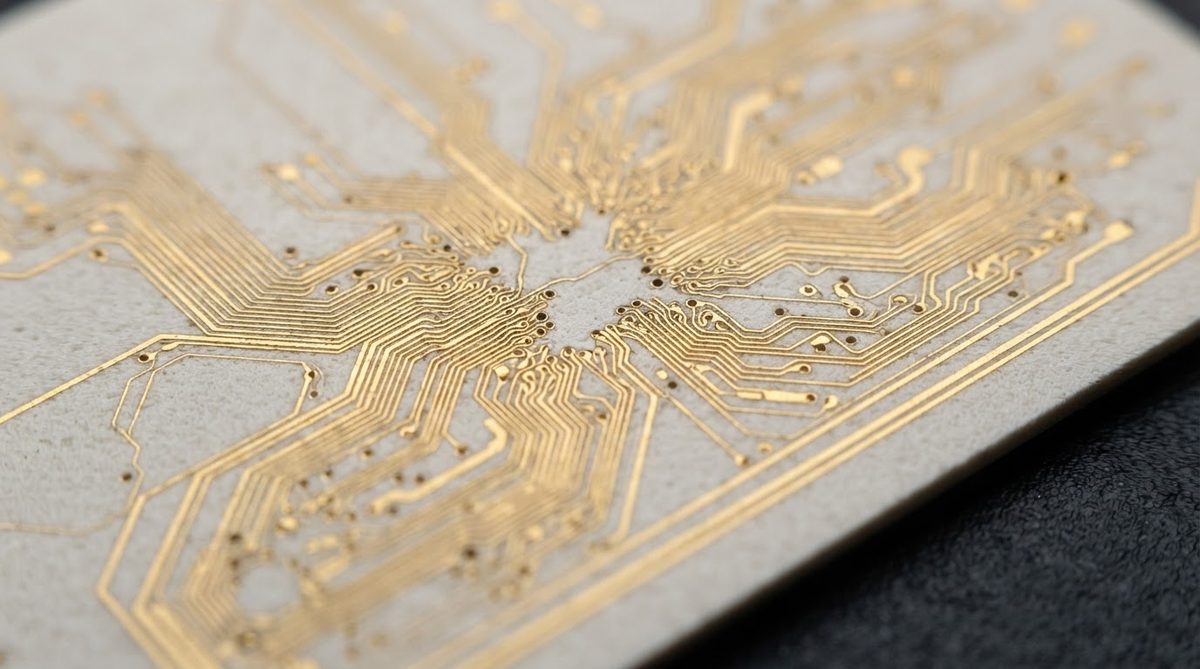
At 0.38 mm thickness, an AlN substrate provides roughly the same thermal resistance as a 2.5 mm thick 96% Al₂O₃ substrate (24–28 W/mK). That ratio matters in stacked assemblies and surface-mount packages where Z-height is constrained. Reducing substrate thickness in alumina below 0.38 mm is possible but introduces fragility problems that AlN handles better thanks to its higher flexural strength at equivalent thickness: 300–350 MPa for AlN versus 250–300 MPa for 96% alumina (three-point bend, ASTM C1161).
CTE match is the second reason engineers choose aluminum nitride AlN thin substrates. Bonding a silicon die to a 96% alumina substrate (CTE 6.5–7.0 ppm/°C) creates a CTE mismatch of roughly 3 ppm/°C. With AlN at 4.5 ppm/°C, that mismatch drops below 1 ppm/°C. Over thousands of thermal cycles, this difference directly reduces solder-joint fatigue and die cracking. If you need help weighing these trade-offs across multiple ceramics, the guide on choosing the right ceramic substrate breaks down the decision framework.
Standard Thickness and Size Options
| Thickness (mm) | Typical Use | Surface Finish (Ra) |
|---|---|---|
| 0.25 | Thin-film resistor networks, MMIC carriers | ≤ 0.05 µm (polished) |
| 0.38 | High-power LED submounts, laser diode mounts | ≤ 0.1 µm (lapped) |
| 0.50 | RF power amplifier bases | ≤ 0.2 µm (as-fired or lapped) |
| 0.635 | IGBT/MOSFET DBC substrates, general power modules | ≤ 0.4 µm (as-fired) |
Typical values for commercially available material, for comparison only. Confirm against the datasheet for your specific grade.
Panel sizes up to 114 × 114 mm are standard from most suppliers (Maruwa, Kyocera, CoorsTek). Larger panels up to 190 × 140 mm are available but carry longer lead times and higher per-piece cost due to sintering yield losses.
Material Properties at a Glance
| Parameter | Value | Unit | Condition | Source |
|---|---|---|---|---|
| Thermal conductivity | 170–200 | W/mK | 25 °C | Maruwa HA-200 datasheet |
| CTE | 4.5–4.7 | ppm/°C | 20–400 °C | Kyocera SH-170 datasheet |
| Dielectric constant (εr) | 8.5–8.9 | — | 1 MHz, 25 °C | CoorsTek ADS-995 |
| Dielectric strength | 15–17 | kV/mm | ASTM D149 | Maruwa HA-200 datasheet |
| Flexural strength | 300–350 | MPa | 3-pt bend, ASTM C1161 | CoorsTek ADS-995 |
| Volume resistivity | > 1014 | Ω·cm | 25 °C | Kyocera SH-170 datasheet |
| Density | 3.26 | g/cm³ | — | Maruwa HA-200 datasheet |
Typical values for commercially available material, for comparison only. Confirm against the datasheet for your specific grade.
Metallization Options for AlN Thin Substrates
Thin-film (sputtered Ti/Pt/Au or TiW/Au): Best for fine-line circuits below 50 µm trace/space. Surface roughness must be ≤ 0.05 µm Ra for good adhesion. This is the standard approach for MMIC carriers and laser submounts. More detail on thin-film processing is available on the AlN thin film ceramic substrate page.
Thick-film (screen-printed tungsten or gold conductors): Used for less demanding line widths (≥ 100 µm). Requires co-firing or post-fire processes. See the AlN thick film ceramic substrate page for specifications.
DBC (direct bond copper): Copper sheets (typically 0.3 mm) bonded to AlN at 1065–1083 °C in a controlled atmosphere. Common for power modules at 0.635 mm substrate thickness. Thinner aluminum nitride AlN thin substrates (0.25–0.38 mm) are rarely used with DBC because the bonding stresses risk warpage or cracking.
Worked Example: Thermal Resistance Through a 0.38 mm AlN Substrate
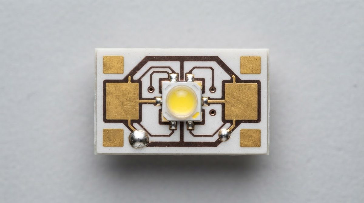
A 5 × 5 mm high-power LED die dissipates 15 W. The AlN substrate is 0.38 mm thick with a thermal conductivity of 180 W/mK.
Thermal resistance through the substrate (one-dimensional approximation):
Rth = t / (k × A) = 0.00038 m / (180 W/mK × 25 × 10⁻⁶ m²) = 0.084 °C/W
Temperature rise across the substrate: ΔT = 15 W × 0.084 °C/W = 1.27 °C.
The same geometry in 96% alumina (k = 26 W/mK) gives Rth = 0.585 °C/W and ΔT = 8.77 °C. That 7.5 °C difference directly extends LED lifetime per Arrhenius derating models. Use the tool below to run this calculation with your own substrate dimensions and power dissipation values.
When Not to Use AlN Thin Substrates
Cost-sensitive, moderate-power designs. If junction temperatures stay below 100 °C with alumina, the 3–5× cost premium of an aluminum nitride AlN thin substrate is hard to justify. Standard 96% Al₂O₃ at 0.635 mm handles most LED and sensor applications adequately.
High mechanical shock or flexure. AlN is a brittle ceramic. For applications with repeated mechanical stress or vibration, silicon nitride (Si₃N₄) thin substrates offer fracture toughness of 6–7 MPa·√m versus AlN’s 2.5–3.0 MPa·√m, at the expense of lower thermal conductivity (70–90 W/mK).
Very large panel sizes. AlN sintering yields drop sharply above ~120 mm in any dimension. For large-area substrates, alumina or metal-core PCBs are more practical.
Humid or unprotected environments. AlN hydrolyzes slowly in the presence of moisture, forming aluminum hydroxide on exposed surfaces. Passivation or hermetic packaging is required for long-term reliability in humid conditions.
Purity and Its Effect on Thermal Performance
AlN substrates are graded primarily by oxygen content in the sintered body. Lower oxygen content yields higher thermal conductivity. A substrate with < 1% oxygen typically achieves ≥ 180 W/mK; substrates with 2–3% oxygen may drop to 150–170 W/mK. Sintering aids (usually Y₂O₃ at 3–5 wt%) form grain-boundary phases that also influence conductivity. For a broader discussion of how purity levels affect ceramic substrate performance, see the article on ceramic substrate purity.
Frequently Asked Questions
Can AlN thin substrates be laser-scribed for snap separation?
Yes. CO₂ and UV lasers can scribe AlN substrates for post-assembly singulation. Scribe depth is typically 30–50% of substrate thickness. Thinner substrates (0.25 mm) require tighter control to avoid through-cuts or micro-cracking along the scribe line.
Does AlN require special storage before metallization?
AlN is hygroscopic at the surface level. Store substrates in sealed, desiccated packaging and process them within 24–48 hours of opening. Surface hydrolysis creates a thin aluminum hydroxide layer that degrades thin-film adhesion if left unchecked.
What solder alloys work on metallized AlN?
AuSn (80/20) is the standard for die-attach on AlN submounts, reflowed at 280–320 °C. SAC305 and SnAgCu alloys work for less critical joints. Avoid high-lead solders above 300 °C reflow on thin substrates without verifying thermal shock tolerance of the specific AlN grade.
How does AlN compare to BeO for thermal performance?
BeO offers 250–300 W/mK, roughly 30–50% higher than AlN. However, beryllium oxide dust is a confirmed human carcinogen and causes chronic beryllium disease, which restricts its use and drives up handling and disposal costs. For most new designs, AlN is the preferred high-conductivity ceramic.
Is AlN compatible with wire bonding?
Yes, provided the metallization stack is appropriate. Au wire bonds to sputtered TiW/Au or Ti/Pt/Au thin films on AlN with pull strengths exceeding 3 gf for 25 µm wire, meeting MIL-STD-883 requirements. Al wedge bonding is also used on Al-metallized AlN substrates.
Next Step
If your thermal model shows that alumina cannot keep junction temperatures within spec, an aluminum nitride AlN thin substrate is the logical next material to evaluate. For volume pricing on standard and custom AlN substrates, visit the AlN ceramic PCB wholesale page or request a quote directly.