A 5G base station PCB AlN PCB substrate is the top choice for power amplifiers and mmWave front-end modules where heat flux exceeds 50 W/cm² and signal integrity above 24 GHz is non-negotiable. Aluminum nitride delivers 170–200 W/mK thermal conductivity, a dielectric constant of 8.5–8.9 at 10 GHz, and a loss tangent below 0.001—numbers that no organic laminate or metal-core PCB can match simultaneously. Engineers evaluating a 5G base station PCB AlN PCB solution will find the specs, worked thermal example, and sourcing guidance they need below.
Key Takeaways
- AlN conducts heat 6–8× better than 96% alumina (24–28 W/mK) and roughly 100× better than FR-4 (0.3 W/mK), critical for GaN HEMT die attach in massive MIMO radios.
- A loss tangent of 0.0003–0.001 at 10 GHz (per Kyocera SN-type AlN datasheet) keeps insertion loss low through mmWave feed networks up to 40 GHz and beyond.
- CTE of 4.4–4.7 ppm/°C closely matches GaN-on-SiC (4.2 ppm/°C) and silicon (2.6–4.1 ppm/°C), reducing solder-joint fatigue during outdoor thermal cycling.
- AlN substrates cost 3–5× more per unit area than 96% alumina; the investment pays off only when thermal or RF performance is the binding constraint.
- Standard AlN ceramic PCBs are available in thicknesses from 0.25 mm to 2.0 mm, with DPC or thin-film metallisation for fine-pitch RF traces.
Why a 5G Base Station PCB AlN PCB Approach Outperforms Alternatives
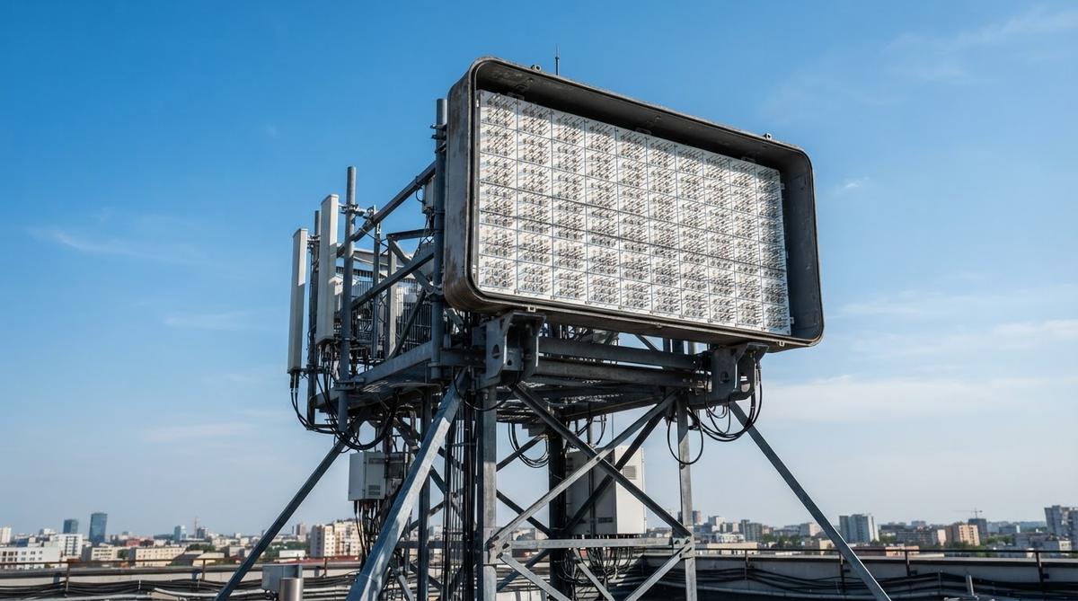
A single 5G massive MIMO active antenna unit (AAU) may pack 64 or more GaN power amplifier (PA) channels into a panel smaller than 0.5 m². Each PA die dissipates 5–15 W in a footprint of a few square millimetres. Organic laminates like Rogers RO4350B handle the RF side reasonably well at sub-6 GHz, but their thermal conductivity (0.6–0.8 W/mK) forces bulky heatsink structures. At mmWave frequencies (24–39 GHz for FR2 bands), dielectric loss in organics rises sharply, and copper roughness on laminate surfaces further degrades insertion loss.
AlN solves both problems in one layer. Its high thermal conductivity pulls heat away from the GaN die to the chassis, and its low loss tangent keeps RF efficiency high. For aerospace and defense radar modules the same logic applies, but 5G infrastructure adds a commercial-volume dimension: a single macro cell site may require hundreds of AlN sub-mounts per AAU.
AlN vs. Alternative Substrates for 5G RF Front Ends
| Parameter | AlN | 96% Al₂O₃ | Rogers RO4350B | Unit | Condition |
|---|---|---|---|---|---|
| Thermal conductivity | 170–200 | 24–28 | 0.69 | W/mK | 20 °C, ASTM E1461 |
| Dielectric constant (εr) | 8.5–8.9 | 9.4–9.8 | 3.48 | — | 10 GHz |
| Loss tangent (tan δ) | 0.0003–0.001 | 0.0001–0.0004 | 0.0037 | — | 10 GHz |
| CTE | 4.4–4.7 | 6.5–7.2 | 10–14 | ppm/°C | 20–300 °C |
| Flexural strength | 300–400 | 300–380 | ~230 (tensile) | MPa | ASTM C1161 / IPC-TM-650 |
| Max continuous use temp. | ~1 000 | ~1 600 | ~250 | °C | In inert / air atmosphere |
Typical values for commercially available material, for comparison only. Confirm against the datasheet for your specific grade. AlN data per Kyocera SN-type and Maruwa HA-series datasheets; Al₂O₃ per CoorsTek ADS-96R; RO4350B per Rogers Corp. datasheet rev. 2023.
Alumina wins on cost and is adequate where per-channel dissipation stays below roughly 2–3 W and frequencies remain under 10 GHz. Rogers laminates are easier to process in standard PCB shops but cannot handle the thermal density of GaN PAs in a compact AAU. For any demanding 5G base station PCB AlN PCB designs fill the gap where both thermal and RF specs are tight.
Thermal Design Example: GaN PA Die on AlN Sub-Mount
Consider a GaN-on-SiC PA die dissipating 10 W over a 3 mm × 3 mm footprint, soldered to a 0.635 mm thick AlN substrate. We estimate the conduction thermal resistance through the substrate alone.
Rth = t / (k × A)
Where t = 0.635 × 10⁻³ m, k = 180 W/mK (mid-range AlN), A = 9 × 10⁻⁶ m².
Rth, AlN = 0.000635 / (180 × 9 × 10⁻⁶) = 0.39 °C/W.
At 10 W dissipation, the temperature drop across the AlN layer is only 3.9 °C. Repeat the same calculation for 96% alumina (k = 26 W/mK): Rth, alumina = 2.72 °C/W, giving a 27.2 °C drop. That 23 °C difference directly extends PA reliability; Arrhenius models for GaN HEMT degradation typically double failure rates for every 15–20 °C rise in junction temperature (per Wolfspeed application note CPWR-AN28).
Enter your substrate area, thickness, and dissipated power below to estimate junction temperature rise for your own 5G base station PCB AlN PCB design.
Metallisation and Trace Design for mmWave
Direct Plated Copper (DPC) and thin-film sputtered metallisation are the two main routes for patterning AlN substrates used in 5G front ends. DPC can achieve trace/space down to 50/50 µm on production panels, sufficient for microstrip and coplanar waveguide (CPW) structures at 28 GHz. Thin-film processes push this below 20/20 µm for tighter integration.
Surface roughness matters at mmWave. Polished or lapped AlN substrates with Ra below 0.05 µm reduce conductor loss from the roughness-dependent skin effect. For feed networks operating above 30 GHz, specify Ra ≤ 0.025 µm and use sputtered gold or copper metallisation to keep insertion loss under 0.1 dB/mm.
Laser scribing enables snap-apart panelisation, which is useful for high-volume 5G sub-mount production. Laser-scribed AlN panels let assemblers populate and reflow an entire panel before singulation, cutting handling costs.
Reliability Under Outdoor Thermal Cycling
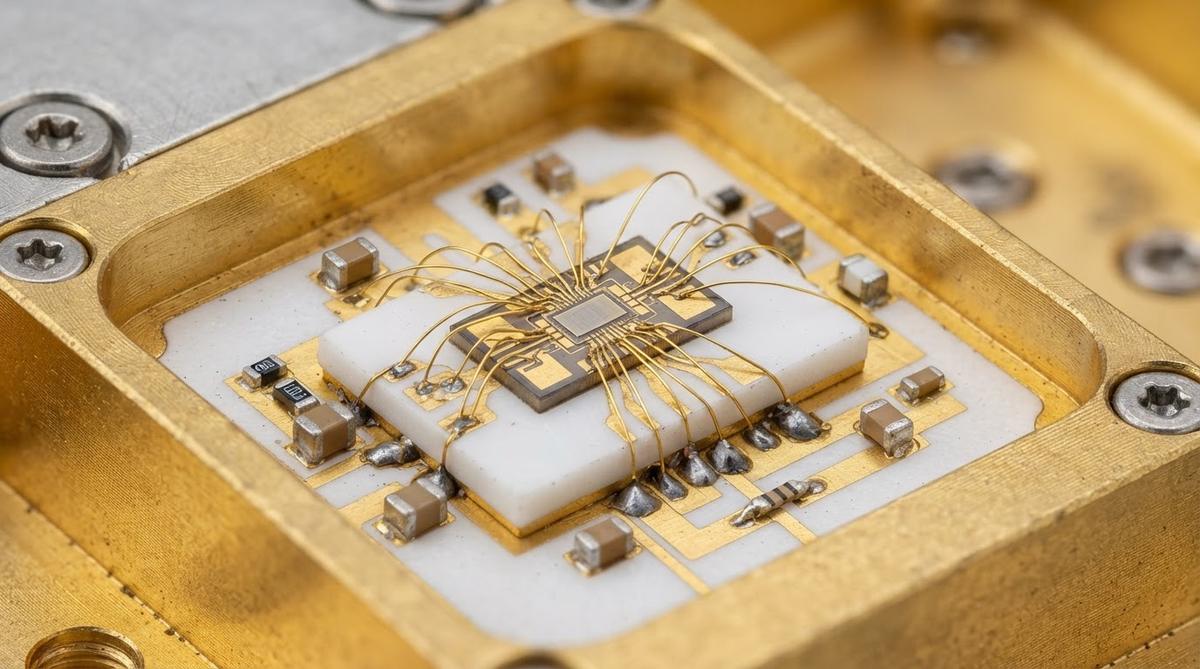
5G macro cell radios sit on towers and rooftops, exposed to ambient swings from −40 °C to +55 °C. With PA self-heating, junction temperatures can reach 150–175 °C. The substrate in any 5G base station PCB AlN PCB assembly must survive thousands of thermal cycles without cracking or delaminating metallisation.
AlN’s CTE of 4.4–4.7 ppm/°C closely matches GaN-on-SiC die (4.2 ppm/°C), so the solder joint between die and substrate sees minimal shear stress. Compare this with an organic laminate at 10–14 ppm/°C: the CTE mismatch drives fatigue cracks in AuSn or SAC305 solder within hundreds of deep cycles. This same CTE advantage benefits automotive electronics on AlN, where under-hood temperatures impose similar cycling demands.
When Not to Use AlN for 5G Base Stations
AlN is overkill—and over-budget—in several common 5G scenarios:
- Sub-6 GHz small cells with per-PA dissipation under 3 W. A standard 96% alumina substrate or even an aluminium-core MCPCB handles the thermal load at a fraction of the cost.
- Digital baseband and control boards. These run at lower frequencies and modest power. FR-4 or high-Tg laminates are appropriate.
- Large-area antenna feed networks at sub-6 GHz. Rogers or Taconic PTFE laminates offer lower εr (3–4 vs. 8.5–8.9), which makes wider traces and easier impedance control for patch antenna arrays.
- Prototype-only runs where lead time matters more than performance. Organic PCBs ship in days; ceramic substrates typically require weeks.
If your thermal budget closes with alumina, choose alumina. A 5G base station PCB AlN PCB premium is justified only when the junction-temperature margin or RF loss budget demands it.
Volume Sourcing for 5G Base Station PCB AlN PCB Projects
5G infrastructure deployments consume AlN substrates in thousands to tens of thousands per product generation. Wholesale AlN substrate sourcing with blanket orders and scheduled releases reduces per-piece cost by 15–30% compared to spot buys. Specify incoming inspection criteria—flatness ≤ 25 µm/25 mm, surface roughness Ra, and dielectric constant tolerance—upfront to avoid lot-to-lot variation that shifts RF tuning.
Frequently Asked Questions
Can AlN substrates handle frequencies above 28 GHz?
Yes. AlN’s loss tangent remains below 0.001 up to at least 40 GHz (per Maruwa HA-series data). Coupled with polished surfaces and thin-film metallisation, AlN supports designs in the 37–40 GHz FR2 bands with acceptable insertion loss.
What solder alloys work for GaN die attach on AlN?
AuSn (80/20) is the standard for high-reliability GaN die attach, offering a solidus of 280 °C and good thermal conductivity (~57 W/mK). SAC305 is used for lower-cost applications but has a lower melting point (217 °C) and slightly worse thermal performance.
How does AlN compare to Si₃N₄ for 5G PA substrates?
Silicon nitride offers superior fracture toughness (6–7 MPa·m^0.5 vs. 2.5–3.5 for AlN) but lower thermal conductivity (70–90 W/mK). For 5G PA sub-mounts where heat extraction is the primary driver, AlN is the better choice. Si₃N₄ is preferred in power modules subject to mechanical shock or high-cycle fatigue.
Is AlN safe to handle and process?
AlN is non-toxic in its sintered ceramic form. Standard ceramic handling precautions—gloves, ESD controls, avoiding mechanical shock—are sufficient. It does not pose the inhalation hazards associated with beryllium oxide ceramics.
What is the typical lead time for AlN PCBs in production volume?
Production lead times for metallised AlN substrates generally range from 3 to 6 weeks depending on metallisation complexity, surface finish, and order quantity. Prototype quantities may ship faster if bare substrates are in stock.
Next Step
If your 5G front-end design requires AlN substrates with DPC or thin-film metallisation, send your Gerber files and thermal requirements for a detailed quotation. AluminaPCB supplies AlN substrates from bare blanks through fully metallised and tested assemblies.