The die attach ceramic substrate combination you choose controls the thermal path from junction to heatsink, sets the upper reliability limit of the package, and constrains your assembly process window. Solder alloys offer a well-understood, moderate-cost path with thermal resistance in the 5–15 K·mm²/W range. Silver sintering drops that to 1–5 K·mm²/W but demands tighter surface prep and higher capital equipment. Conductive epoxy is the simplest to process yet thermally the weakest, typically 30–80 K·mm²/W. The right choice depends on die power density, operating temperature, and production volume.
Key Takeaways
- Ag sinter bond lines achieve thermal conductivity of 150–250 W/mK—close to bulk silver—making them the best thermal option for high-power die attach on AlN or Si₃N₄ ceramic substrates.
- AuSn (80/20) solder reflows at 280 °C and survives continuous operation above 200 °C, but costs roughly 8–12× more per gram than SAC305.
- Conductive epoxy cures below 200 °C and needs no flux, but its thermal conductivity (1–5 W/mK) limits it to die dissipating under ~2 W.
- Ceramic surface finish—metallisation type, roughness, and flatness—affects bond-line void fraction more than the attach material itself.
- Void content above 5 % in the bond line can raise local thermal resistance by 20–40 %, per Infineon application note AN2019-03.
Why the Die Attach Ceramic Substrate Pairing Matters
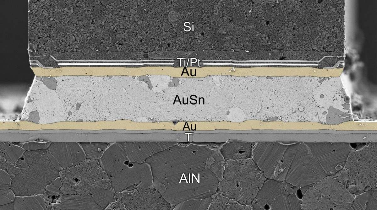
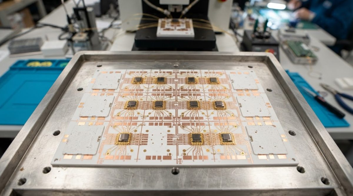
Ceramic substrates used for die attach fall into three main families: alumina (Al₂O₃), aluminum nitride (AlN), and silicon nitride (Si₃N₄). Each has a different CTE, surface energy, and metallisation chemistry, all of which influence wetting, adhesion, and long-term fatigue life of the bond. A detailed comparison of types of ceramic substrates is useful background before selecting an attach method.
AlN’s CTE of 4.5 ppm/°C closely matches silicon (2.6 ppm/°C) and SiC (4.0 ppm/°C), reducing shear stress in the solder joint during thermal cycling. Alumina at 96 % purity has a CTE of ~7.1 ppm/°C—still far lower than FR-4 (~14 ppm/°C)—but the mismatch with SiC die is large enough to limit solder joint life under aggressive cycling (ΔT > 150 °C). Si₃N₄ offers the highest fracture toughness (6–8 MPa·√m per CoorsTek SN-88 datasheet) and is the preferred die attach ceramic substrate for IGBT and power module applications where mechanical shock and thermal cycling coexist.
Surface finish is equally critical. A sputtered Ti/Ni/Au or Ti/Pt/Au stack on a lapped ceramic surface (Ra < 0.2 µm) will wet with AuSn solder to near-zero void levels. A thick-film Ag pad on an as-fired surface (Ra 0.4–0.8 µm) traps more flux residue and generates higher void fractions. If your substrate needs tighter surface control, review specifications for lapping and polishing ceramic PCBs.
Solder Die Attach on Ceramic Substrates: Alloys, Process, and Limits
Solder is the most common die attach method on ceramic substrates. The alloy choice depends on operating temperature, cost, and RoHS compliance.
Common Solder Alloys for Ceramic Die Attach
| Alloy | Liquidus (°C) | Thermal Conductivity (W/mK) | Max Service Temp (°C) | Relative Cost | Source |
|---|---|---|---|---|---|
| AuSn 80/20 | 280 | 57 | ~250 | High | Indium Corp. datasheet |
| AuGe 88/12 | 356 | 44 | ~300 | Very high | Indium Corp. datasheet |
| SAC305 (Sn96.5Ag3Cu0.5) | 217–220 | 58–62 | ~150 | Low | IPC J-STD-006C |
| SnPb 63/37 (legacy) | 183 | 50 | ~125 | Low | IPC J-STD-006C |
| SnSb 95/5 | 232–240 | ~26 | ~175 | Low–Med | Kester datasheet |
Typical values for commercially available material, for comparison only. Confirm against the datasheet for your specific grade.
AuSn 80/20 is the workhorse for GaN HEMTs, laser diodes, and other die that run above 150 °C continuously. It forms a eutectic joint at 280 °C in a nitrogen or forming-gas atmosphere, requires no flux when used with clean Au-finished surfaces, and produces void levels below 2 % with proper preform placement. The penalty is gold cost: a 3 mm × 3 mm preform at 25 µm thickness contains roughly 5.6 mg of Au.
SAC305 is adequate for die running below 125 °C in consumer or industrial applications. It is RoHS-compliant, cheap, and compatible with standard reflow ovens. However, its creep resistance degrades rapidly above 100 °C, and thermal cycling life on a die attach ceramic substrate with large CTE mismatch is limited.
Worked Example: Bond-Line Thermal Resistance
Assume a 5 mm × 5 mm SiC MOSFET die soldered to an AlN DBC substrate with AuSn at a bond-line thickness of 25 µm and 3 % void fraction.
Effective thermal conductivity, accounting for voids: k_eff ≈ k_solder × (1 − void%) = 57 × 0.97 = 55.3 W/mK.
Thermal resistance of the bond line: R_th = t / (k_eff × A) = 25 × 10⁻⁶ / (55.3 × 25 × 10⁻⁶) = 0.018 K/W.
That 0.018 K/W is a small fraction of the total junction-to-case resistance (typically 0.3–0.8 K/W for a packaged SiC device). But if voids climb to 15 %, R_th rises to ~0.021 K/W and—more critically—local hot spots under the void can push junction temperature 10–20 °C above the average, accelerating electromigration and solder fatigue.
Enter your substrate area, thickness, and dissipated power below to estimate junction temperature rise for your own die attach ceramic substrate design.
Silver Sinter Die Attach
Silver sintering bonds a die to a substrate using nano- or micro-scale Ag particles in a paste or film, pressed and heated (typically 230–280 °C at 10–30 MPa for pressure-assisted sintering). The resulting bond is >95 % dense silver with a thermal conductivity of 150–250 W/mK and a melting point of 961 °C—far above any realistic operating temperature.
This makes Ag sinter the preferred attach for SiC and GaN power devices operating above 200 °C, where even AuSn joints begin to creep. Heraeus, Henkel, and Kyocera all publish paste datasheets showing shear strengths of 30–60 MPa after sintering, compared to 20–40 MPa for AuSn solder.
The trade-offs are real. Pressure-assisted sintering requires a precision press, die-level alignment, and careful control of temperature ramp rate. Capital cost for a production sintering press starts around $300k–$500k. Pressureless sinter pastes exist but achieve lower density (80–90 %) and correspondingly lower thermal conductivity (100–150 W/mK). The substrate must have an Ag or Au finish; Ni-finished pads require an additional plating step. Substrate flatness below 5 µm/10 mm is strongly recommended to achieve uniform pressure across the die.
Conductive Epoxy Die Attach
Silver-filled conductive epoxies (e.g., Henkel Ablestik 84-1LMISR4, AI Technology AIT Cool-Bond) cure at 125–175 °C and bond to nearly any metallised or bare ceramic surface. They are the simplest process: dispense, place die, oven cure. No flux, no inert atmosphere, no pressure.
Thermal conductivity is the limitation. Even premium Ag-filled epoxies reach only 2–5 W/mK—roughly 10–25× worse than AuSn solder. This restricts epoxy attach to low-power die: sensors, small-signal ICs, MEMS, photodetectors, and RF die dissipating under ~2 W on a ceramic carrier. For those applications, epoxy is often the most cost-effective and mechanically forgiving option, especially on alumina 96 % thick-film substrates where pad geometry is less precise.
Head-to-Head Comparison of Die Attach Methods on Ceramic Substrates
| Parameter | AuSn Solder | Ag Sinter (pressure) | Ag Epoxy | Unit |
|---|---|---|---|---|
| Bond-line thermal conductivity | 57 | 150–250 | 2–5 | W/mK |
| Process temperature | 280–320 | 230–280 | 125–175 | °C |
| Applied pressure | 0 (reflow) | 10–30 | 0 | MPa |
| Shear strength (on Au pad) | 20–40 | 30–60 | 5–15 | MPa |
| Max continuous service temp | ~250 | >300 | 150–200 | °C |
| Void fraction (typical) | 2–5 | 1–5 | 5–15 | % |
| Relative material cost per die (3×3 mm) | $$ | $ | $ | — |
| Capital equipment cost | Low–Med | High | Low | — |
Typical values for commercially available material, for comparison only. Confirm against the datasheet for your specific grade.
Choosing the Right Die Attach Ceramic Substrate Method: A Decision Fork
Die power density above 100 W/cm² or operating temperature above 200 °C? Use Ag sinter on AlN or Si₃N₄. The thermal and reliability margin justifies the process complexity. Many Si₃N₄ substrate suppliers now offer pre-metallised blanks optimised for sinter attach.
Die power density 10–100 W/cm², operating temperature 125–200 °C? AuSn solder on AlN or high-purity alumina. Well-characterised, high yield, and no press needed.
Die power density below 10 W/cm², operating temperature below 150 °C? Conductive epoxy on alumina. Lowest process cost, adequate thermal path, and the ceramic substrate’s own thermal spreading dominates the total resistance.
If you are still scoping substrate options, the effect of ceramic purity on performance directly influences which attach methods are viable on a given die attach ceramic substrate.
When NOT to Use a Ceramic Substrate for Die Attach
Ceramic substrates are not always the right answer. If the die dissipates less than 0.5 W and the operating environment stays below 85 °C, a standard FR-4 or metal-core PCB with epoxy attach is cheaper and mechanically simpler. Ceramic is brittle; if the assembly will see high mechanical shock (>1500 g) without potting or structural support, consider a flex-rigid or metal carrier instead. For very large substrate areas (>100 mm × 100 mm) at low power density, the cost premium of ceramic over aluminium MCPCB is hard to justify.
FAQ
Can I solder directly to bare alumina without metallisation?
No. Bare alumina does not wet with any standard solder alloy. You need a metallisation layer—typically sputtered Ti/Ni/Au, thick-film Ag/Pd, or DBC copper—before soldering. Active brazing alloys containing titanium (e.g., Incusil-ABA) can bond to bare ceramic, but these are brazing processes at 800+ °C, not die attach.
Does silver sinter paste require a gold-finished substrate?
Most Ag sinter pastes are qualified on Ag or Au surface finishes. Some newer formulations (e.g., Heraeus ASP295) are validated on bare Cu with oxide control, but shear strength and reliability data on Cu are less mature. Check the paste vendor’s qualification report for your specific finish.
What void level is acceptable for a die attach on ceramic?
MIL-STD-883 Method 2030 specifies a maximum of 50 % voiding for standard applications and 25 % for power devices. In practice, most automotive and power module OEMs set internal limits of 5–10 %. X-ray or scanning acoustic microscopy (SAM) is the standard inspection method per JEDEC JESD22-A104.
How does CTE mismatch affect die attach reliability on ceramic?
CTE mismatch between die and substrate creates cyclic shear stress in the bond line during temperature swings. A larger mismatch (e.g., Si on Al₂O₃: ~4.5 ppm/°C delta) shortens fatigue life. Coffin-Manson models predict that doubling the CTE mismatch roughly halves the number of cycles to failure for a given ΔT, assuming the same bond-line thickness and material.
Can I rework a die attached to a ceramic substrate?
Solder-attached die can be reworked by reheating above liquidus, but ceramic substrates are brittle and sensitive to thermal shock. Use a localised hot-gas nozzle, not a full-board reflow. Epoxy-attached die can sometimes be sheared off mechanically, but this risks cracking the substrate. Ag-sintered joints are extremely strong and are generally considered non-reworkable without destroying the substrate metallisation.
Is die attach paste the same as solder paste?
No. Die attach paste is formulated for single-die or small-area dispensing with controlled bond-line thickness, and often uses different flux chemistries or no flux at all. Standard SMT solder paste is designed for stencil printing across a full board and is not optimised for void-free die attach. Use a paste specifically qualified for die attach by the vendor.
For substrate sourcing, download ceramic substrate datasheets to compare material grades before committing to an attach method. If you are ready to prototype, request a quote through the ceramic PCB manufacturing page to discuss metallisation and finish options with an engineer.