Yes, ceramic PCBs can be reworked, but only within narrow limits. The substrate is brittle, the metallisation is thin, and the thermal mass is high relative to FR-4. A standard hot-air rework station can crack a 0.635 mm alumina board if the operator heats one corner while the opposite corner stays cold. Successful ceramic PCB rework demands controlled, uniform heating, the right tools, and a clear understanding of what is repairable and what is not.
Key Takeaways
- Single-component rework on ceramic substrates succeeds reliably when the entire board is preheated to within 50–80 °C of the solder liquidus before local reflow.
- Thick-film (screen-printed) metallisation tolerates 3–5 reflow cycles before adhesion degrades measurably, per typical vendor data (Kyocera, CoorsTek thick-film application notes).
- Thin-film and DPC metallisation layers are 1–10 µm thick; aggressive solder tip contact or abrasive cleaning can destroy a trace in seconds.
- Multilayer ceramic boards (HTCC/LTCC) with embedded vias are effectively non-repairable at the internal layer level.
- For high-reliability programmes (aerospace, implantable medical), rework is usually prohibited by the quality plan; replacement is the only option.
Why Ceramic PCB Rework Is Harder Than FR-4 Rework
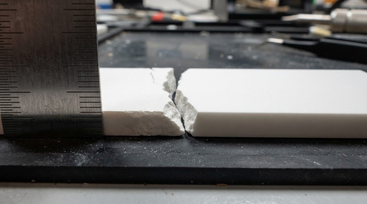
FR-4 is a glass-epoxy composite. It flexes. Ceramic does not. Alumina (Al₂O₃) has a flexural strength of 300–380 MPa (per ASTM C1161), which sounds high until you remember it has near-zero plastic deformation. Any bending stress beyond the elastic limit causes immediate fracture, not gradual yielding. During rework, the most common source of bending stress is thermal gradient across the board.
The coefficient of thermal expansion (CTE) of 96% alumina is about 7.1 ppm/°C (20–300 °C range, per CoorsTek ADS-96R datasheet). If one zone of a 50 × 50 mm substrate reaches 250 °C while the opposite edge is still at 25 °C, the differential expansion creates enough tensile stress on the cool side to initiate a crack from any existing edge flaw. This is the single biggest cause of rework-induced ceramic failure.
Rework Methods That Work on Ceramic Substrates
Whole-board preheat plus localised reflow
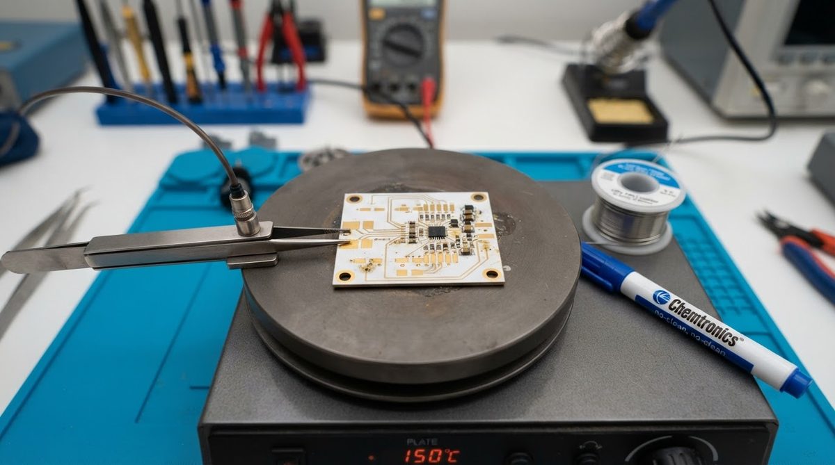
The safest approach uses a bottom-side IR or convection preheater to bring the entire board to 150–180 °C, then applies a focused hot-air nozzle or micro-soldering iron to the target component. Keeping the thermal gradient below 2–3 °C/mm across the substrate virtually eliminates fracture risk. Most ceramic rework stations in power-module production lines follow this profile.
Vapour-phase (condensation) soldering for full reflow
If every component needs replacement, vapour-phase soldering offers the most uniform heating. The board cannot exceed the boiling point of the heat-transfer fluid (typically 230 °C for Galden LS/230 or 260 °C for HS/260), which protects against overshoot. This method is common in prototype rework of multilayer ceramic PCB assemblies where selective heating is impractical.
Laser-assisted desoldering
A diode laser (808–980 nm) focused on a single pad can melt solder in under 2 seconds with minimal heat spread. This works well on thin-film and DPC boards where the metallisation is too thin to survive prolonged iron contact. The equipment cost limits this to high-value assemblies.
What You Can and Cannot Repair
| Repair Type | Feasibility | Notes |
|---|---|---|
| Replace a surface-mount passive (0402–2512) | Routine | Preheat required; standard rework station |
| Replace a QFN or BGA | Possible with care | Reballing and stencil needed; X-ray inspection after |
| Replace a power die (sintered or soldered) | Difficult | Die-attach voiding risk high on second attach; may need vacuum reflow |
| Repair a cracked substrate | Not feasible | No adhesive restores dielectric strength or thermal path |
| Repair a delaminated thick-film trace | Not feasible | Re-screen and re-fire is a full remanufacture, not a repair |
| Repair an internal via in HTCC/LTCC | Not feasible | Internal layers are co-fired; no access without destroying the board |
| Add a jumper wire for an ECO | Possible | Bond wire or fine magnet wire; must be mechanically secured |
Typical assessment for commercially available ceramic PCBs. Confirm against your specific metallisation type and quality requirements.
Worked Example: Thermal Gradient Check Before Rework
Suppose you need to replace a 5 × 5 mm QFN on a 25.4 × 25.4 × 0.635 mm 96% alumina board. The solder is SAC305 (liquidus 217–220 °C). Your hot-air nozzle heats a 10 mm diameter zone.
Step 1. Set the bottom preheater to 170 °C. Wait until the board surface reads 160–165 °C on a thermocouple taped to the far corner.
Step 2. The nozzle needs to add roughly 55 °C locally (from 165 °C to 220 °C). Over a 10 mm radius, this creates a gradient of about 55 °C / 10 mm = 5.5 °C/mm at the boundary.
Step 3. That gradient is above the 2–3 °C/mm guideline. Options: use a wider nozzle (15 mm), raise the preheat to 190 °C (reducing the delta to 30 °C), or slow the ramp rate so heat conducts outward before the centre peaks. Alumina’s thermal conductivity of 24–28 W/mK helps here; a 3-second dwell at 200 °C before ramping to 220 °C often suffices.
This kind of quick calculation, done before you turn on the station, prevents most rework-induced cracks. Understanding your ceramic PCB manufacturing capabilities and metallisation type also informs how many reflow cycles the board can tolerate.
How Many Times Can You Rework a Ceramic Board?
Thick-film metallisation (fired at 850 °C) is inherently stable through multiple solder reflows at 220–260 °C. Adhesion testing per IPC-TM-650 2.4.21 typically shows less than 10% peel-strength degradation after 5 reflow cycles. Thin-film sputtered metallisation (Ti/Pt/Au or Ti/Ni/Au) is more sensitive; intermetallic growth between the solder and the barrier layer accumulates with each cycle. Three reflows is a practical limit for thin-film boards in critical applications.
DBC (direct bond copper) substrates handle thermal cycling well because the copper layer is 0.3 mm thick, but the ceramic-to-copper bond can fatigue after repeated high-ΔT excursions. If you are reworking a DBC-based power module, keep records of every thermal cycle the board has seen.
When NOT to Rework a Ceramic PCB
Replace instead of rework when any of these apply:
- The substrate is cracked, chipped, or has visible edge damage. No rework saves a fractured ceramic.
- The board is part of a Class 3 (high-reliability) assembly governed by IPC-6012 or equivalent. Most aerospace and medical quality plans prohibit rework on ceramic substrates entirely.
- The failure is in an internal layer of an HTCC or LTCC stack. There is no non-destructive way to access buried conductors.
- The metallisation has lifted or blistered. Re-adhesion is not possible without re-firing, which means remanufacturing the board.
- The cost of the rework station time exceeds the cost of a new board. For standard 96% alumina substrates, a single-layer board may cost less than the labour for a careful rework. Check 96% alumina ceramic PCB pricing before committing to a repair.
Handling and ESD Precautions During Rework
Ceramic substrates are excellent insulators, which means they hold static charge readily. Always work on a grounded ESD mat, wear a wrist strap, and ionise the air near the board. Dropping a ceramic board even 20 mm onto a hard surface can chip an edge, creating a stress riser that propagates during the next thermal cycle. Use vacuum tweezers or padded fixtures, not finger grip. For guidance on safe transport after rework, see ESD-safe packaging and shipping of ceramic boards.
Frequently Asked Questions
Can you solder to a ceramic PCB with a regular soldering iron?
Yes, but only with preheat. A soldering iron applies heat to one point, creating a steep thermal gradient. Preheat the board to at least 150 °C on a hot plate first, then use a fine-tip iron with a controlled temperature setting. Avoid pressing down on the board.
Does rework void the warranty on a ceramic PCB?
Most ceramic PCB manufacturers warrant the bare board, not the assembly. Once components are soldered, the board warranty typically ends. Rework does not change this, but it may void your assembly house’s workmanship warranty. Check both contracts.
Can I use flux remover on a ceramic substrate?
Standard IPA-based and hydrocarbon flux removers are safe on bare ceramic and on most thick-film metallisations. Avoid aggressive halogenated solvents on thin-film boards, as they can attack the adhesion layer. Always test on a scrap coupon first.
Is it possible to re-ball a BGA on a ceramic interposer?
Yes. The process is the same as for organic substrates: remove residual solder, apply flux, place new solder spheres with a stencil, and reflow. The key difference is that the ceramic interposer must be uniformly preheated to avoid cracking. Vapour-phase reflow works well for this.
What inspection should follow a ceramic board rework?
At minimum, perform visual inspection under 10× magnification for substrate cracks and solder joint quality. For BGA or hidden-joint components, X-ray inspection is necessary. Electrical continuity and hipot testing confirm that the dielectric integrity of the substrate was not compromised.
Next Step
If your project involves ceramic boards that may need rework during prototyping, factor that into your choice of ceramic PCB manufacturer. Ask whether they supply rework guidelines specific to their metallisation process. For a quote on replacement boards or prototype quantities, visit the ceramic PCB FAQ or request pricing directly.