Proper PCB packaging ESD shipping practice is essential for ceramic substrates because the boards are both brittle and carry ESD-sensitive metallisation. A single uncontrolled discharge above 100 V can damage thin-film traces, while a 30 cm drop onto a hard surface can crack an alumina substrate. Standard pink poly bags and bubble wrap are not enough. This article covers the materials, procedures, and inspection checks that keep ceramic boards intact from factory to assembly line.
Key Takeaways
- Thin-film ceramic circuits (DPC, sputtered metallisation) can be damaged by human-body-model (HBM) discharges as low as 100-200 V; thick-film circuits tolerate roughly 500-2,000 V depending on trace geometry.
- 96% alumina has a flexural strength of 300-380 MPa (per ASTM C1161), but zero ductility means any point load concentrates stress into a fracture.
- ESD shielding bags (per ANSI/ESD S541) must have a surface resistivity of 1 × 10³ to 1 × 10¹¹ Ω/sq to qualify as static-dissipative or shielding.
- Vacuum-sealed trays with foam inserts reduce in-transit breakage rates to below 0.1% on shipments tested across major express carriers.
- Incoming inspection should include a visual check for edge chips, a continuity test on critical nets, and humidity indicator card verification.
Why PCB Packaging ESD Shipping Matters for Ceramics
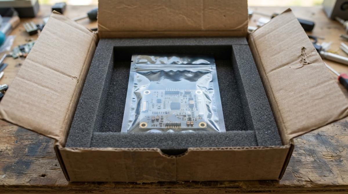
FR-4 boards flex. Ceramic boards do not. A 0.635 mm alumina substrate snaps under bending loads that a 1.6 mm FR-4 panel absorbs without damage. This brittleness makes mechanical packaging just as important as ESD control in any PCB packaging ESD shipping workflow.
On the electrical side, ceramic substrates are excellent insulators (volume resistivity >10¹⁴ Ω·cm for Al₂O₃). That means triboelectric charge generated during handling stays on the surface instead of bleeding away. Without a controlled discharge path, voltage builds until it arcs across fine-pitch traces. DPC metallisation with 50 µm line/space is especially vulnerable. Even boards with wider thick-film conductors can suffer micro-melting at pad edges from an HBM event.
ESD-Safe Packaging Materials for Ceramic Boards
Three layers of protection are standard practice for PCB packaging ESD shipping, each serving a distinct function.
| Layer | Material | Function | Key Spec | Reference |
|---|---|---|---|---|
| Inner wrap | Static-dissipative foam or conductive foam insert | Cushions substrate, drains charge | Surface resistivity 1 × 10⁵ – 1 × 10⁹ Ω/sq | ANSI/ESD S541 |
| Barrier bag | Moisture-barrier, ESD-shielding bag (metallised polyester laminate) | Faraday cage effect blocks external fields; moisture barrier protects finishes | Shielding: <50 nJ per MIL-PRF-81705 Type III | MIL-PRF-81705 |
| Outer box | Double-wall corrugated carton with rigid foam inserts | Absorbs drop and vibration energy | Edge crush test ≥ 48 lb/in (ASTM D5639) | ASTM D5639 |
Typical values for commercially available materials, for comparison only. Confirm against the datasheet for your specific grade.
Pink polyethylene bags are antistatic (they reduce triboelectric generation) but do not provide shielding. They are acceptable as an inner wrap for thick-film boards shipped short distances, but they should never be the only ESD layer for thin-film or high-value assemblies.
Step-by-Step Packing Procedure
- Wear a grounded wrist strap and work on an ESD-safe mat. Verify the strap’s resistance is between 750 kΩ and 10 MΩ per ANSI/ESD S1.1.
- Inspect each board visually under 5× magnification for edge chips, cracks, or delamination before packing. Reject any board with a chip deeper than 0.1 mm into the substrate edge.
- Place a humidity indicator card (HIC) and a desiccant sachet (per IPC/JEDEC J-STD-033D) inside the bag if the surface finish is ENIG, ENEPIG, or bare copper. Target <10% RH inside the sealed bag.
- Seat each board into a custom-cut conductive foam tray. The cavity should match the board outline within ±0.5 mm so the substrate cannot shift. For thin substrates (≤0.38 mm), use a full-perimeter ledge support rather than a bottom-only pocket.
- Slide the loaded tray into a moisture-barrier ESD shielding bag. Vacuum-seal or heat-seal the bag closed.
- Place the sealed bag into a rigid inner box with at least 25 mm of closed-cell foam on all six sides.
- Pack the inner box into the shipping carton with additional void fill. The board should survive ISTA 2A transit testing (a sequence of drops, vibration, and compression) without cracking.
Use the tool below to check whether your substrate material needs temperature derating that could affect packaging material selection—some foams lose cushioning performance above 60 °C.
Shipping Considerations by Carrier and Distance
Express air freight subjects packages to pressure changes (cabin altitude equivalent to ~2,400 m) and conveyor impacts at sorting hubs. Vacuum-sealed bags may inflate slightly at altitude; leave 10-15% headspace in the outer carton to accommodate this. Ground freight adds sustained vibration in the 5-200 Hz range per ASTM D4169, which can cause micro-abrasion if boards contact each other.
For international shipments, label the outer carton with the ESD-sensitive device symbol per IEC 60417-5134 and the fragile symbol per ISO 7000-0621. Customs inspectors who open the package must be instructed (via a printed insert) not to remove boards from their ESD bags. If your boards ship from overseas suppliers, review the ceramic PCB sourcing and supply chain to understand handoff points where packaging integrity is most at risk.
Incoming Inspection After Receiving
Even well-packed boards can arrive damaged. A brief receiving inspection catches problems before they reach the assembly line.
- Check the HIC. If the 10% dot has turned pink, moisture ingress occurred. Bake the boards per J-STD-033D before soldering.
- Visual inspection at 10×. Look for corner chips, hairline cracks radiating from via holes, and discolouration on exposed copper.
- Continuity / isolation spot check. Probe at least two critical nets per board. Measure isolation resistance between adjacent pads; it should exceed 100 MΩ at 50 VDC for ceramic substrates.
Understanding how boards are fabricated helps you set realistic acceptance criteria. The PCB manufacturing process from Gerber to finished board explains where dimensional and cosmetic variation originates.
When NOT to Use Standard ESD Bags

Standard ESD shielding bags are the wrong choice in several situations. If your ceramic board includes exposed wire-bondable gold pads, the metallised inner surface of a shielding bag can scratch the bond surface. Use a rigid waffle tray with a conductive lid instead. If the board is larger than 150 × 150 mm and thinner than 0.5 mm, bag packaging allows too much flexing during handling. Ship these in vacuum-formed JEDEC-style trays.
For assemblies with tall components already soldered to the ceramic substrate, foam inserts must be custom-profiled. Off-the-shelf packaging will apply point loads to component leads and risk cracking solder joints or the substrate itself.
When Ceramic-Specific PCB Packaging ESD Shipping Is Overkill
If you are shipping standard 1.6 mm FR-4 boards with conformal coating, the full ceramic packaging protocol described here adds unnecessary cost. FR-4 tolerates bending and minor impacts. Pink poly bags with standard corrugated boxes and basic ESD labels are sufficient for most FR-4 shipments per IPC-1601. Reserve the rigid-tray, vacuum-seal, double-box method for ceramic substrates, bare die carriers, and other brittle or high-value assemblies.
Matching Packaging to Substrate Material
Different ceramic materials have different fracture toughness values, which affects how aggressively you need to pack them. Tailoring your PCB packaging ESD shipping approach to the specific substrate avoids both under-protection and unnecessary cost.
| Material | Fracture Toughness (K_IC) | Unit | Packaging Implication | Source |
|---|---|---|---|---|
| Al₂O₃ 96% | 3.5–4.0 | MPa·m^½ | Standard rigid tray + shielding bag | CoorsTek datasheet |
| AlN | 2.5–3.5 | MPa·m^½ | Extra foam; avoid point contact on edges | Kyocera SH-15 datasheet |
| Si₃N₄ | 6.0–7.0 | MPa·m^½ | Most forgiving ceramic; standard tray is adequate | Kyocera SN-88 datasheet |
Typical values for commercially available material, for comparison only. Confirm against the datasheet for your specific grade.
AlN substrates deserve the most caution. Their lower fracture toughness means edge chips propagate into full cracks more easily. If your design uses AlN for aerospace and defence applications, specify MIL-PRF-81705 Type III shielding bags and ISTA 3A transit testing in your packaging requirements.
FAQ
Can I reuse ESD bags for ceramic PCBs?
Yes, if the bag passes a surface resistivity check (1 × 10³ – 1 × 10¹¹ Ω/sq) and has no punctures or creases that compromise the shielding layer. Metallised shielding bags degrade after 3-5 uses. Test before each reuse with a surface resistance meter per ANSI/ESD STM11.11.
Do ceramic PCBs need nitrogen backfill in the sealed bag?
Only if the metallisation is bare copper or bare silver and the expected shelf life exceeds 6 months. For ENIG or gold-finished boards, desiccant and vacuum sealing are sufficient. Nitrogen backfill adds cost and requires a gas-flush sealer.
What drop height should my PCB packaging ESD shipping setup survive?
ISTA 2A specifies drops from 76 cm for packages under 10 kg. For ceramic PCBs, design your inner foam to keep peak deceleration below 50 G at that height. A simple calculation: 25 mm of 2.0 lb/ft³ polyethylene foam compresses roughly 60% before bottoming out, which limits a 0.5 kg payload to about 40 G at 76 cm drop height.
Should I ground the outer shipping carton?
No. The outer carton is an insulator by design. Grounding it would require a conductive surface, which creates new discharge risks during handling. The Faraday cage effect of the inner shielding bag is the correct protection layer. Keep the outer box as a mechanical shell only.
How do I label ceramic PCB shipments for customs?
Apply the ESD-sensitive device symbol (IEC 60417-5134) and “FRAGILE” (ISO 7000-0621) on at least two sides. For international shipments, include the HS code for your specific product and a packing list that describes the contents as “ceramic printed circuit boards.” Review the tariff and country-of-origin guide for ceramic PCBs for classification details.
Next Step
If you are specifying PCB packaging ESD shipping requirements for an upcoming ceramic board order, include your needs in the RFQ. Suppliers who understand ceramic PCB manufacturing can match tray design and bag selection to your substrate material, thickness, and metallisation type. Request a quote at AluminaPCB.com and note your packaging preferences in the comments field.