Immersion silver (IAg) deposits 0.05–0.40 µm of pure silver onto exposed copper pads through a chemical displacement reaction, producing a flat, solderable surface that costs less than ENIG and delivers comparable coplanarity. On ceramic substrates—Al₂O₃, AlN, or Si₃N₄—immersion silver works well for fine-pitch soldering and high-frequency circuits, but its limited shelf life and susceptibility to tarnish require careful handling and storage protocols.
Key Takeaways
- Immersion silver thickness on ceramic PCBs typically ranges from 0.10 to 0.30 µm per IPC-4553A, with a minimum of 0.08 µm for acceptable solderability.
- Shelf life before assembly is 6–12 months when vacuum-sealed with sulfur-free interleaving paper, versus 1–3 months if stored in open air.
- IAg is 30–50% cheaper per panel than ENIG for equivalent pad counts, making it attractive for cost-sensitive production runs.
- Silver migration under DC bias and humidity can cause dendritic shorts at spacings below 0.15 mm—a real concern in high-density ceramic designs.
- For wire bonding or long-term storage, ENIG or ENEPIG are better choices; immersion silver is optimized for reflow soldering within a controlled timeline.
What Is Immersion Silver and How Does It Work on Ceramic PCBs?
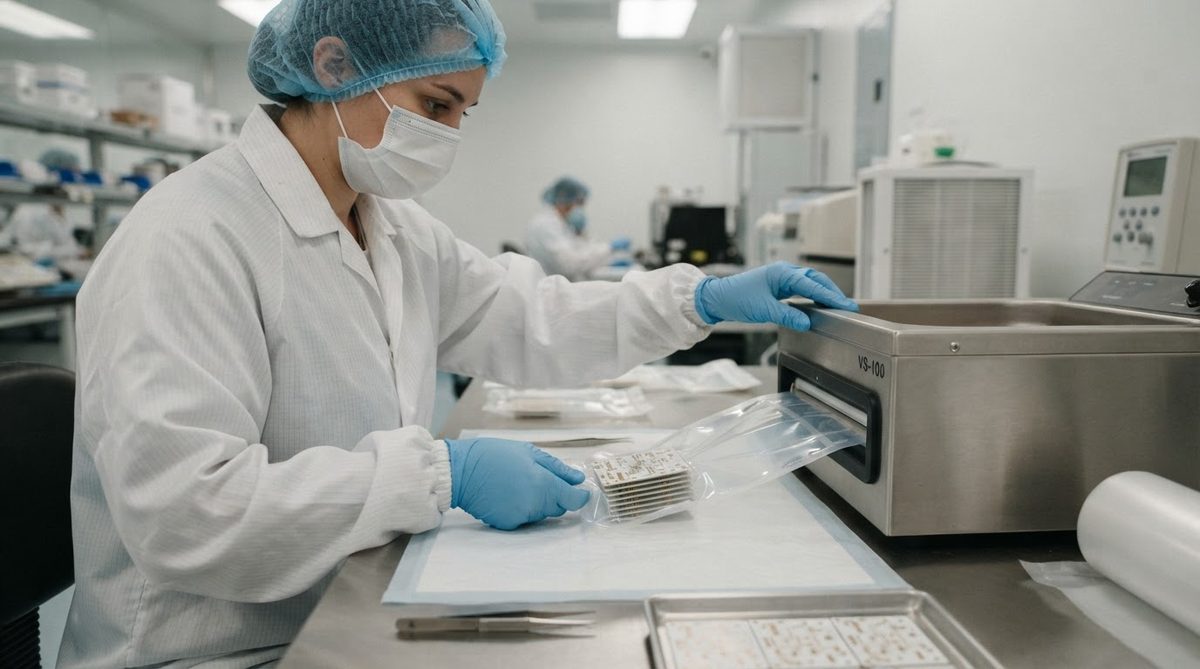
Immersion silver is a surface finish applied by dipping copper-metallized ceramic substrates into an acidic silver ion bath. The process relies on galvanic displacement: copper atoms on the pad surface dissolve into solution while silver ions plate out in their place. The reaction is self-limiting—once the copper surface is fully covered, deposition slows and stops, producing a thin, uniform silver layer.
On ceramic PCBs, the underlying substrate is inert. Unlike FR-4, there is no resin to absorb moisture or outgas during the plating bath, which simplifies process control. The copper layer on a ceramic board is typically applied by ceramic PCB manufacturing methods such as DPC (direct plated copper) or thick-film metallization. Immersion silver adheres to this copper regardless of the deposition method, provided the copper surface is properly cleaned and micro-etched before plating.
Most immersion silver baths also deposit an organic anti-tarnish layer simultaneously. This co-deposited organic barrier slows sulfur and chlorine attack on the silver surface, extending the window for assembly.
Immersion Silver Thickness and Specification
IPC-4553A defines the requirements for immersion silver finishes. The standard specifies a minimum silver thickness of 0.08 µm for solderability, but most fabricators target 0.10–0.30 µm for production boards. Thicker deposits (up to 0.40 µm) are possible but offer diminishing returns: the self-limiting reaction makes uniform deposits above 0.30 µm difficult to achieve without modified chemistries.
| Parameter | Value | Unit | Condition | Source |
|---|---|---|---|---|
| Silver thickness (min) | 0.08 | µm | Per IPC-4553A | IPC-4553A |
| Silver thickness (typical) | 0.10–0.30 | µm | Production target | IPC-4553A |
| Silver purity | ≥ 99.0 | % | Weight basis | IPC-4553A |
| Surface roughness (Ra) | 0.1–0.3 | µm | After plating | Typical process data |
| Contact angle (solderability) | < 30 | degrees | SAC305, 245 °C, fresh finish | IPC J-STD-003C |
| Shelf life (vacuum-sealed) | 6–12 | months | Sulfur-free packaging | Industry practice |
Typical values for commercially available material, for comparison only. Confirm against the datasheet for your specific grade.
Why Choose Immersion Silver on a Ceramic Substrate?
Immersion silver offers three advantages that matter on ceramic boards:
Coplanarity. The finish is extremely flat—pad-to-pad height variation is typically under 5 µm. This matters for fine-pitch BGAs and QFNs on alumina or AlN substrates where the ceramic itself is ground flat to tight tolerances. A finish that adds height variation would negate the substrate’s planarity advantage.
High-frequency performance. Silver has the highest electrical conductivity of any metal (6.30 × 10⁷ S/m at 20 °C). At microwave frequencies, current flows in the skin depth—roughly 0.64 µm at 10 GHz in silver. Even a 0.20 µm immersion silver layer reduces RF insertion loss compared to ENIG, where the nickel barrier layer (3–6 µm, conductivity only 1.43 × 10⁷ S/m) sits directly in the signal path. For ceramic materials used in RF applications, this is a meaningful difference.
Cost. Silver chemistry is simpler and faster than electroless nickel/immersion gold. Bath costs are lower, and cycle times are shorter—typically 30–90 seconds of immersion versus 15–25 minutes for the full ENIG process.
Cost Comparison: Immersion Silver vs. Other Ceramic PCB Finishes
The cost gap between finishes depends on board size, pad count, and gold price. As a rough guide, immersion silver adds $0.02–$0.05 per cm² to the bare board cost, while ENIG adds $0.04–$0.10 per cm². OSP is cheaper still but offers a narrower process window. Use the estimator below to compare finish costs for your specific board dimensions and pad density.
[pcb_calc type=”finish-cost”]
For a 25 × 25 mm AlN substrate with 120 pads, switching from ENIG to immersion silver typically saves 25–40% on the finishing step. Over a 1,000-piece production run, that saving can offset a meaningful portion of the ceramic substrate premium. However, you must factor in the cost of sulfur-free packaging and any tighter inventory controls needed to manage shelf life. OSP on ceramic substrates is even cheaper per panel but limited to a single reflow pass in most cases.
Tarnish, Handling, and Shelf Life
Silver tarnishes. Atmospheric sulfur compounds—H₂S, COS, and organic sulfides—react with silver to form Ag₂S, a dark, non-solderable film. Chlorine exposure produces AgCl. Both degrade solderability rapidly.
Practical countermeasures:
- Vacuum-seal boards immediately after finishing, using sulfur-free desiccant and interleaving paper. Standard cardboard contains sulfur compounds and will tarnish boards within days.
- Store at < 30 °C, < 60% RH. Elevated temperature and humidity accelerate tarnish formation exponentially.
- Wear nitrile gloves during handling. Latex gloves can contain sulfur-based vulcanizing agents that transfer to the surface on contact.
- Assemble within 24 hours of opening the vacuum pack in a production environment. If that is not feasible, re-seal with nitrogen purge.
If your assembly line cannot guarantee these controls, immersion tin for ceramic PCBs or ENIG may be more forgiving choices. Immersion tin has its own shelf-life constraints (tin whisker risk over 6+ months), but it does not tarnish visibly the way silver does.
Silver Migration: The Real Risk at Fine Pitch
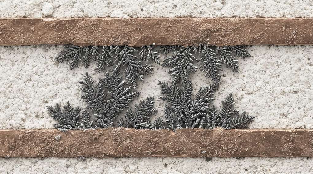
Electrochemical migration (ECM) is the primary reliability concern with immersion silver. Under DC bias and humidity, silver ions dissolve at the anode pad, migrate through surface moisture, and re-deposit as metallic dendrites at the cathode pad. These dendrites can bridge adjacent traces and cause intermittent or permanent shorts.
The risk scales with three factors: applied voltage, humidity, and trace spacing. At 0.10 mm pitch under 85 °C / 85% RH with 5 V DC bias, silver migration can produce dendrites within 100–500 hours per published SIR (surface insulation resistance) test data. At 0.30 mm pitch under the same conditions, mean time to failure extends beyond 1,000 hours.
Conformal coating after assembly largely eliminates the moisture pathway and is standard practice for ceramic assemblies in automotive and industrial environments. If your design operates in a sealed, dry enclosure, migration risk drops substantially even without coating.
When NOT to Use Immersion Silver on Ceramic PCBs
Wire bonding. Gold or aluminum wire bonding requires a hard, bondable surface—typically ENIG, ENEPIG, or electrolytic gold. Immersion silver does not provide a reliable wire bond interface.
Long storage before assembly. If boards will sit in inventory for more than 6 months before soldering, the tarnish risk makes immersion silver a liability. ENIG or ENEPIG are better for boards with uncertain assembly timelines.
High-humidity, uncoated operation. Outdoor sensors, marine electronics, or any application where the finished assembly will see sustained humidity above 80% RH without conformal coating should avoid exposed silver traces. Consider ceramic PCB surface finishes with better corrosion resistance such as ENIG or ENEPIG.
Ultra-fine pitch below 0.10 mm with DC bias. The silver migration risk at these spacings is difficult to mitigate even with conformal coating. ENIG or OSP are safer for sub-0.10 mm geometries under bias.
Frequently Asked Questions
Can immersion silver survive multiple reflow cycles?
Yes, immersion silver can withstand 2–3 lead-free reflow cycles (peak 260 °C) with acceptable solderability, provided the boards are stored properly between passes. Beyond three cycles, wetting performance degrades noticeably as the thin silver layer dissolves into the solder.
Does immersion silver work on aluminum nitride substrates?
It works on any copper-metallized ceramic substrate, including AlN. The silver plating reacts with the copper layer, not the ceramic. The substrate material is irrelevant to the finish chemistry, though AlN boards used in UV LED applications may need additional tarnish protection due to elevated operating temperatures.
How do I tell if immersion silver has tarnished too much to solder?
A light yellow or straw tint is normal and still solderable. A brown, purple, or dark gray discoloration indicates Ag₂S formation and poor wettability. If in doubt, run a solder spread test per IPC J-STD-003C before committing to a production run.
Is immersion silver RoHS-compliant?
Yes. Immersion silver contains no restricted substances under RoHS Directive 2011/65/EU. Silver is not on the SVHC candidate list under REACH. The finish is fully compatible with lead-free assembly.
What is the difference between immersion silver and electroplated silver?
Immersion silver is a thin (0.08–0.40 µm), self-limiting displacement deposit. Electroplated silver uses external current to build thicker layers (1–25 µm) and is used for contacts, connectors, and RF waveguide surfaces. Electroplated silver costs more and requires masking but provides better wear resistance and lower RF loss at high power.
Next Step
If immersion silver fits your assembly timeline and operating environment, it is one of the most cost-effective finishes for ceramic PCBs. Review the ceramic PCB fabrication capabilities page to confirm compatibility with your substrate and metallization, then request a quote with your finish specified.