Ceramic substrates (Al₂O₃, AlN, Si₃N₄) conduct heat 10–100× better than borosilicate or fused-silica glass, tolerate higher operating temperatures, and survive harsher mechanical loads. Glass substrates cost less per unit area, transmit light, and offer very low dielectric loss at mmWave frequencies. The right choice depends on whether your design is thermally limited, optically dependent, or cost-constrained.
Key Takeaways
- 96% alumina delivers 24–28 W/mK thermal conductivity; borosilicate glass delivers roughly 1.1 W/mK—a 20× gap that matters for any power-dissipating component.
- Glass substrates achieve dielectric loss tangent (tan δ) values below 0.001 at 10 GHz, making them competitive with LTCC for low-loss RF signal routing.
- Ceramic substrates operate continuously above 800 °C; most electronic-grade glasses soften between 500–700 °C (strain point), limiting high-temperature use.
- Glass panel processing (fan-out, TGV) scales to large panels (≥ 500 × 500 mm), reducing per-unit cost for high-density interposer and display-adjacent applications.
- Ceramic is brittle but stronger in flexure (300–400 MPa for 96% Al₂O₃ per ASTM C1161) than borosilicate glass (≈ 70 MPa).
What Counts as a “Glass Substrate” in Electronics?
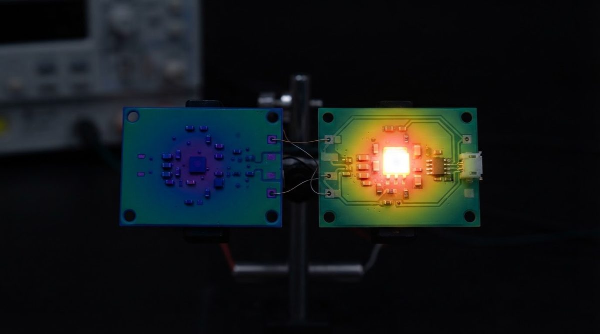
In this comparison, “glass” means flat, amorphous silicate panels used as circuit substrates—borosilicate (Schott AF 32, Corning Eagle XG), fused silica, or alkali-free display glass repurposed for packaging and RF. These are not the same as glass-ceramic composites used in LTCC cofired multilayers, which behave more like ceramics after sintering.
“Ceramic substrate” here covers polycrystalline alumina (Al₂O₃ 96% and 99.6%), aluminum nitride (AlN), and silicon nitride (Si₃N₄). These are sintered from powder, opaque, and metallised with thick-film, thin-film, DPC, or DBC processes.
Property-by-Property Comparison: Ceramic vs Glass Substrate
| Parameter | 96% Al₂O₃ | AlN | Borosilicate Glass | Fused Silica | Unit | Condition | Source |
|---|---|---|---|---|---|---|---|
| Thermal conductivity | 24–28 | 170–200 | 1.1–1.2 | 1.3–1.5 | W/mK | 20 °C | CoorsTek ADS-996, Kyocera SH-30; Schott AF 32 datasheet |
| CTE | 7.0–7.4 | 4.5–4.8 | 3.2–3.3 | 0.5–0.6 | ppm/°C | 20–300 °C | Same sources |
| Dielectric constant (εᵣ) | 9.4–9.8 | 8.5–9.0 | 4.6–5.1 | 3.7–3.8 | — | 1 MHz | Kyocera; Schott; Corning |
| Loss tangent (tan δ) | 0.0002–0.001 | 0.0003–0.001 | 0.0005–0.001 | 0.0001–0.0002 | — | 1–10 GHz | Same sources |
| Flexural strength | 300–400 | 300–350 | 60–70 | 50–65 | MPa | ASTM C1161 / ISO 14704 | CoorsTek; Schott |
| Max continuous use temp. | 1 600 | 1 000 | 500 (strain pt.) | 1 000 | °C | In air, no load | Manufacturer datasheets |
| Optical transparency | Opaque | Opaque | > 90% (visible) | > 90% (UV–visible) | % | 1 mm thickness | Schott; Corning |
| Typical substrate cost | 1× | 3–5× | 0.3–0.5× | 0.5–1× | relative | 100 × 100 mm panel | Industry pricing, 2024 |
Typical values for commercially available material, for comparison only. Confirm against the datasheet for your specific grade.
Thermal Management: Where Ceramic Wins Outright
Any design that must spread or sink heat through the substrate needs ceramic. A 10 W LED mounted on a 25 × 25 × 0.635 mm 96% alumina substrate sees a conductive thermal resistance of roughly:
Rth = t / (k × A) = 0.000635 / (26 × 0.000625) = 0.039 °C/W
The same geometry in borosilicate glass (k ≈ 1.1 W/mK):
Rth = 0.000635 / (1.1 × 0.000625) = 0.923 °C/W
At 10 W dissipation, that difference is 0.39 °C vs 9.2 °C across the substrate alone. For power electronics, LED arrays, and laser diode submounts, this gap eliminates glass from contention. If your thermal budget is tight, compare DBC vs DPC ceramic metallisation rather than switching to glass.
RF and mmWave: Where Glass Gets Interesting
Glass substrates have a lower dielectric constant (εᵣ ≈ 4.6–5.1 for borosilicate vs 9.4–9.8 for alumina). Lower εᵣ means wider traces for a given impedance, which relaxes fabrication tolerances and reduces conductor loss at frequencies above 20 GHz. Fused silica pushes εᵣ below 3.8 with tan δ under 0.0002, approaching quartz performance at lower cost.
For 5G mmWave antenna-in-package (AiP) modules running at 28–39 GHz, glass interposers from suppliers like Corning and AGC are gaining traction. The combination of low loss, large panel size, and through-glass via (TGV) capability makes glass competitive with LTCC for passive antenna redistribution layers—provided the package does not also need to sink significant heat.
Ceramic still wins for high-power RF. GaN HEMT carriers dissipating tens of watts per device need AlN or at minimum 96% alumina. The substrate must conduct heat, not just route signals.
CTE Matching: A Nuanced Trade-Off
Silicon die CTE is about 2.6 ppm/°C. Borosilicate glass (3.2–3.3 ppm/°C) matches silicon more closely than alumina (7.0–7.4 ppm/°C). This tighter CTE match reduces solder-joint stress during thermal cycling for bare-die flip-chip attach—one reason glass interposers are used in advanced semiconductor packaging.
AlN (4.5–4.8 ppm/°C) offers a reasonable middle ground: better CTE match to silicon than alumina, with far superior thermal conductivity. For power module designs comparing these, see the ceramic substrate comparison hub.
Mechanical Strength and Handling
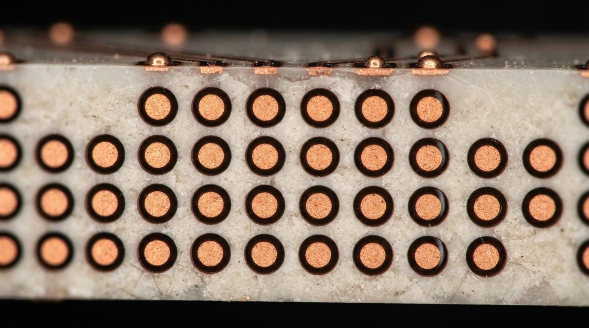
Both materials are brittle, but ceramic is substantially stronger. A 96% alumina substrate withstands 300–400 MPa in four-point bending (per ASTM C1161). Borosilicate glass reaches roughly 60–70 MPa under the same test. In practice, glass substrates thinner than 0.3 mm require careful handling fixtures and are more prone to edge chipping during dicing and pick-and-place.
If your assembly line already handles FR-4 and you are moving to a hard substrate for the first time, ceramic is more forgiving of minor handling errors than glass.
When NOT to Use Ceramic (Choose Glass Instead)
Glass is the better substrate when:
- Optical transparency is required. Biosensor windows, display-adjacent interposers, and photonic packages need light transmission that ceramic cannot provide.
- Large-panel, low-cost fan-out packaging is the goal. Glass panel processing on 500 × 500 mm or larger panels drives per-unit cost well below ceramic, which is typically processed on panels ≤ 190 × 190 mm.
- Very tight CTE match to silicon matters more than thermal conductivity—e.g., passive interposers with no significant heat dissipation.
- Ultra-low εᵣ at mmWave is the primary electrical requirement and power density is low.
Conversely, if your board dissipates more than a few watts, operates above 500 °C, or faces mechanical shock, ceramic is the safer choice. For a cost perspective on ceramic versus organic alternatives, see ceramic PCB vs metal-core PCB.
Process Compatibility
Ceramic substrates accept thick-film screen printing, thin-film sputtering, DPC (direct plated copper), DBC (direct bonded copper), and AMB (active metal brazing). These are mature, high-reliability metallisation routes with decades of field history in automotive and aerospace.
Glass substrates are metallised primarily by sputtering and semi-additive plating (SAP). Through-glass vias (TGVs) are formed by laser drilling or photoetch, then filled with copper. The TGV process is still scaling; via density and reliability data are less mature than ceramic via technologies. If you need a proven multilayer ceramic process, DPC vs thin-film metallisation is a more relevant comparison.
FAQ
Can glass substrates handle lead-free soldering?
Yes. Lead-free reflow peaks at roughly 260 °C, well below the strain point of borosilicate glass (≈ 500 °C). Standard SAC305 profiles work on glass substrates without deformation, though thermal shock sensitivity requires slower ramp rates than ceramic.
Is glass cheaper than ceramic for prototypes?
Not necessarily at prototype volumes. Glass panel processing is cost-effective at scale (thousands of units on large panels), but small-batch glass substrates with TGVs can cost as much as alumina DPC boards. Ceramic prototyping has shorter lead times at most fabricators.
Do glass substrates work for power LEDs?
Only for very low-power LEDs (under ~0.5 W per device). The thermal conductivity of borosilicate glass (1.1 W/mK) creates a thermal bottleneck that raises junction temperature and shortens LED life. Use alumina or AlN for any LED dissipating more than 1 W.
What is the thinnest glass substrate available for electronics?
Corning and Schott offer electronic-grade glass as thin as 0.1 mm (100 µm). Handling at this thickness requires vacuum chucks and carrier bonding. Ceramic substrates are typically available down to 0.25 mm (250 µm) before handling becomes impractical.
Can I use glass in a hermetic package?
Glass-to-metal seals are well established for hermetic feedthroughs, but an all-glass hermetic package is uncommon. Ceramic (alumina or AlN) brazed or soldered lids remain the standard for hermetic enclosures in military and space applications per MIL-STD-883.
Next Step
If thermal conductivity is a primary requirement, ceramic is almost certainly the right substrate. Review the AMB vs DPC process comparison to narrow down your metallisation, then request a quote with your design files at AluminaPCB’s instant quote page.