An RF microwave PCB built on ceramic typically costs 3–10× more per unit area than an equivalent FR-4 or PTFE-based board. Most of that rf microwave pcb pcb cost premium is driven by substrate material, metallization method, and the tight dimensional tolerances microwave circuits demand. Understanding where the money goes lets you make trade-offs that cut cost without sacrificing electrical performance.
Five Drivers Behind RF Microwave PCB PCB Cost
Every ceramic RF board quote is shaped by the same handful of variables. Rank-ordered by impact on unit price, they are:
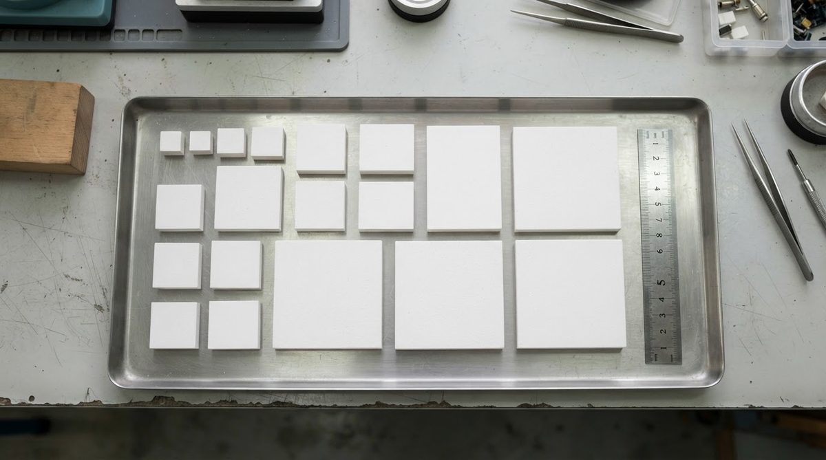
- Substrate material and grade. 96% alumina (Al₂O₃) is the workhorse for circuits up to about 20 GHz and the least expensive ceramic option. 99.6% alumina offers lower surface roughness and tighter dielectric tolerance, but costs roughly 1.5–2× more per blank. Aluminum nitride (AlN) is chosen when thermal conductivity matters alongside RF performance, adding another 3–5× over 96% alumina. For detailed pricing on advanced substrates, see silicon nitride ceramic PCB pricing.
- Metallization process. Thick-film screen printing is the lowest-cost route and suits many designs below 6 GHz. Thin-film sputtering (Ti/Pt/Au, TaN, NiCr) is required for tight impedance control, fine lines, and frequencies above 10 GHz, but it adds 2–4× to the metallization step alone.
- Line width and spacing. A 50 Ω microstrip on 254 µm alumina at 10 GHz needs a trace width around 240 µm. Push that to 75 µm traces for a coupled-line filter at 40 GHz, and you move from screen printing into thin-film photolithography with tighter process controls and lower yields.
- Dimensional and dielectric tolerance. Standard alumina substrates hold εr to ±0.3 (roughly ±3% at εr ≈ 9.8). Specifying ±0.1 means sorting or premium-grade blanks, both of which raise cost.
- Panel utilization and quantity. Ceramic substrates are fired as individual blanks or small panels, not large-format sheets. Odd board outlines or large keep-out areas waste material quickly. Volume pricing kicks in above roughly 100–500 pieces depending on complexity.
Thin Film vs. Thick Film: Where RF Microwave PCB PCB Cost Splits
The metallization choice is often the single largest cost decision on an RF ceramic PCB. Here is a direct comparison.
| Parameter | Thick Film | Thin Film | Unit / Condition |
|---|---|---|---|
| Typical min. line/space | 100–125 | 10–25 | µm |
| Conductor metals | Ag, AgPd, Au | Au, Cu, TaN, NiCr | — |
| Sheet resistance tolerance | ±10–15% | ±1–2% | of nominal |
| Impedance repeatability (50 Ω line) | ±3–5 Ω | ±0.5–1 Ω | board-to-board |
| Relative metallization cost | 1× | 2–4× | per substrate |
| Typical frequency ceiling | ~6–10 GHz | 40 GHz+ | practical limit |
Typical values for commercially available processes, for comparison only. Confirm against the datasheet for your specific grade.
For designs operating below 6 GHz with 50 Ω microstrip widths above 150 µm, thick-film ceramic processing delivers acceptable performance at a fraction of the rf microwave pcb pcb cost. Above 10 GHz, or wherever you need integrated thin-film resistors for bias networks and terminations, thin-film processing becomes necessary despite its higher price.
Worked Example: Cost Per Channel for a 10 GHz LNA Module
Consider a two-stage low-noise amplifier on a 25.4 mm × 12.7 mm × 0.254 mm 99.6% alumina substrate with thin-film gold metallization, two sputtered NiCr resistors, and ENIG finish pads for die attach.
- Substrate blank (99.6% Al₂O₃, polished): ~$3–5 per piece at 250-piece volume.
- Thin-film metallization (Ti/Pt/Au, photolithography, etch): ~$8–15 per piece at 250-piece volume.
- Laser trim of integrated resistors: ~$1–2 per piece.
- Final inspection and RF test coupon: ~$0.50–1 per piece.
Total ceramic substrate cost lands around $12–23 per board at prototype-to-low-volume quantities. In contrast, the same footprint on Rogers RO4003C laminate with standard PCB processing might cost $1–3 per board, but will not match the thermal stability, hermeticity, or long-term drift performance alumina provides in a sealed module.
At production volumes of 5,000+ pieces, thin-film ceramic pricing drops 30–50% through panel batching and amortized tooling. The gap versus organic laminates narrows considerably once you factor in the cost of rework, field failures, and the hermetic package the ceramic substrate enables. This volume effect is one of the most overlooked aspects of rf microwave pcb pcb cost planning.
Enter your substrate dimensions, material, and metallization type below to get a rough cost estimate for your RF board.
[pcb_calc type=”pcb-quote”]
How to Reduce RF Microwave PCB PCB Cost Without Hurting Performance
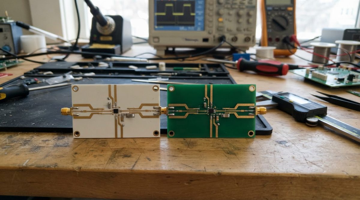
Use 96% alumina unless you have a measured reason not to. At frequencies below 20 GHz, the dielectric loss difference between 96% and 99.6% alumina (tan δ ≈ 0.0002 vs. 0.0001 at 10 GHz, per CoorsTek ADS-96R and ADS-996 datasheets) rarely justifies the price jump. Reserve 99.6% for circuits where insertion loss budgets are razor-thin.
Relax tolerances where the circuit allows it. A 50 Ω feed line connecting two components does not need ±0.5 Ω impedance control. Specify tight tolerances only on resonant structures, coupled lines, and matching networks.
Design for standard blank sizes. Ceramic substrates are available in standard dimensions (25.4 × 25.4 mm, 50.8 × 50.8 mm, etc.). Fitting your layout to a standard blank avoids custom scribing charges. Panelizing multiple circuits on one blank further improves utilization.
Consolidate resistor values. Every unique thin-film resistor value that requires laser trimming adds cycle time. Designing bias networks with fewer distinct resistance values reduces trim cost.
When Not to Use a Ceramic Substrate for RF
Ceramic is not the right call for every microwave board. Choose a PTFE or hydrocarbon laminate (Rogers RO4000 series, Taconic TLY) when:
- The operating frequency is below 6 GHz and thermal dissipation is under 2 W.
- Board area exceeds roughly 100 × 100 mm. Large ceramic panels are expensive and fragile to handle.
- The product is consumer-grade with a target BOM cost under $5 for the entire assembly.
- You need plated through-holes for multilayer routing. Ceramic vias (punched or laser-drilled) cost more than standard PTH in organic laminates.
For a broader view of how ceramic compares across applications, the complete ceramic PCB cost guide covers material, process, and volume trade-offs in detail.
Frequently Asked Questions
Is ceramic always more expensive than Rogers laminates for RF?
Yes, on a per-board basis ceramic substrates cost more than Rogers or Taconic PTFE laminates. The rf microwave pcb pcb cost premium ranges from 3× for simple thick-film alumina boards to 10× or more for thin-film AlN substrates. The cost gap shrinks at higher volumes and in applications where ceramic eliminates a separate hermetic package.
What is the minimum order quantity for RF ceramic PCBs?
Most ceramic PCB fabricators accept orders as low as 5–25 pieces for prototypes. Per-piece pricing at these volumes is high because tooling and setup costs are spread across few units. Budget 30–50% cost reduction when moving to 500+ pieces.
Can I mix thick-film and thin-film on the same RF ceramic board?
Yes, hybrid processing is common. A typical approach uses thick-film conductors for ground planes and low-frequency interconnects, then adds thin-film resistors and precision transmission lines in a second metallization step. This reduces cost compared to full thin-film processing while maintaining RF performance where it matters.
Does surface roughness affect RF ceramic PCB cost?
It does. Standard as-fired alumina has a surface roughness (Ra) of 0.3–0.8 µm. Polishing to Ra < 0.05 µm for millimeter-wave thin-film circuits adds $1–3 per substrate at volume. The smoother surface reduces conductor loss at frequencies above 20 GHz, so the spend is justified for Ka-band and above.
How does via cost compare between ceramic and organic RF boards?
Ceramic vias are formed by punching or laser drilling green tape before firing (HTCC/LTCC) or by laser drilling and filling fired substrates. Either method costs 2–5× more per via than a standard plated through-hole in FR-4 or Rogers laminate. Minimizing via count is one of the most effective ways to control ceramic RF board cost. For designs where dense via arrays are unavoidable, semiconductor packaging ceramic substrates offer optimized via grid pricing.