Semiconductor packaging PCB cost ranges from roughly $2.50 to $40+ per unit for a 25 × 25 mm ceramic substrate, depending on material (Al₂O₃, AlN, or Si₃N₄), metallization method (DBC, AMB, DPC, thin film, or thick film), and the dimensional tolerances your die-attach process demands. That makes ceramic 5–50× more expensive per unit area than FR-4. A 96% alumina DBC substrate in production volumes of 5,000+ pieces typically lands between $2.50 and $6.00 per unit; the same footprint in AlN with thin-film metallization can reach $15–$40.
Key Takeaways
- Substrate material alone accounts for 30–60% of total semiconductor packaging PCB cost; AlN is 3–5× the price of 96% alumina per unit area.
- Metallization process choice (DBC vs. AMB vs. thin film vs. thick film) can swing unit cost by 2–4× for the same substrate.
- Tighter line/space requirements below 75 µm push you toward thin-film or DPC processes, adding $5–$20 per piece at prototype quantities.
- Volume is the strongest lever: moving from 100-piece prototypes to 10,000-piece production often cuts unit cost 40–60%.
- Si₃N₄ substrates offer superior mechanical reliability for power-cycling applications but carry a significant price premium over both alumina and AlN.
What Drives Semiconductor Packaging PCB Cost?
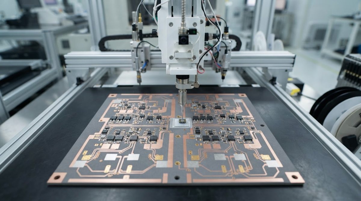
Semiconductor packages demand more from a substrate than a typical circuit board. The die-attach area needs flatness under 25 µm, CTE must be close enough to silicon (2.6 ppm/K) or the die material to survive thermal cycling, and the metallization must support wire bonding or solder reflow at 260–320 °C. Each of these requirements has a direct cost consequence.
The table below maps the primary cost drivers to their typical impact. Use it as a checklist when scoping a new package design.
| Cost Driver | Low-Cost Choice | High-Cost Choice | Typical Cost Impact |
|---|---|---|---|
| Substrate material | Al₂O₃ 96% | Si₃N₄ | 3–10× per unit area |
| Metallization | Thick film (screen print) | Thin film (sputter + etch) | 2–4× |
| Copper thickness | ≤ 0.3 mm (DBC) | ≥ 0.6 mm (AMB) | 1.3–2× |
| Line/space | ≥ 150 µm | ≤ 50 µm | 1.5–3× |
| Surface finish | Bare Cu + OSP | Electroless NiPdAu | +$0.50–$2.00/pc |
| Via density | No vias | Filled vias, laser drilled | +30–80% |
| Volume | 10,000+ pcs | 50 pcs prototype | 5–10× per unit |
Estimates based on typical market pricing for 25 × 25 mm substrates, 2024–2025. Confirm with your supplier for exact quotes.
Substrate Material: The Biggest Line Item
Material selection is often locked in by the thermal and mechanical requirements of the semiconductor die, leaving little room to negotiate. Still, understanding the price tiers helps you push back on over-specification.
| Material | Thermal Conductivity (W/mK) | CTE (ppm/K, 25–400 °C) | Relative Cost (Al₂O₃ 96% = 1×) | Source |
|---|---|---|---|---|
| Al₂O₃ 96% | 24–28 | 7.0–7.4 | 1× | CoorsTek ADS-996 datasheet |
| Al₂O₃ 99.6% | 30–35 | 7.2–7.6 | 1.5–2× | Kyocera A-493 datasheet |
| AlN | 170–200 | 4.5–5.0 | 3–5× | Maruwa HA-200 datasheet |
| Si₃N₄ | 70–90 | 2.5–3.5 | 6–10× | CeramTec Rocar SN datasheet |
Typical values for commercially available material, for comparison only. Confirm against the datasheet for your specific grade.
For most IGBT and MOSFET packages dissipating under 100 W, 96% alumina with DBC metallization is the cost-effective baseline. AlN becomes justified when junction-to-case thermal resistance must drop below roughly 0.3 °C/W for the given die size, or when CTE mismatch with the die would cause solder-joint fatigue in fewer than the required power cycles. Si₃N₄ substrate pricing reflects both raw material cost and the difficulty of machining and metallizing this material, but its fracture toughness (6–7 MPa·m½ vs. 3–4 for AlN) can eliminate field failures that cost far more than the substrate premium.
Metallization Process and Its Cost Impact
The metallization method determines both the minimum feature size and the bond strength to the ceramic. In semiconductor packaging, the two dominant approaches are DBC (direct bond copper) for power modules and thin film for RF/MMIC and fine-pitch die attach.
DBC bonds a copper foil (typically 0.15–0.6 mm) to the ceramic through a Cu–O eutectic layer at roughly 1,065 °C. It is well-suited to high-current paths but limited to line/space around 150 µm minimum. AMB (active metal brazing) uses a Ti-containing braze and can bond thicker copper to AlN or Si₃N₄ with better adhesion, at a 30–80% cost premium over DBC on the same substrate. For a deeper look at the cost differences between print-and-fire and sputter-etch approaches, see the breakdowns for thick-film ceramic cost and thin-film ceramic cost.
Thin-film metallization (sputter Ti/Pt/Au or Ti/Cu/Ni/Au, then photolithographically pattern) achieves line/space down to 10–25 µm. This is essential for MMIC packaging and flip-chip bumping but adds significant per-piece cost due to vacuum deposition, photoresist, and etch steps. Expect $10–$25 per piece for a 25 × 25 mm AlN thin-film substrate at 500-piece volumes.
Worked Example: Estimating Cost for a SiC MOSFET Package
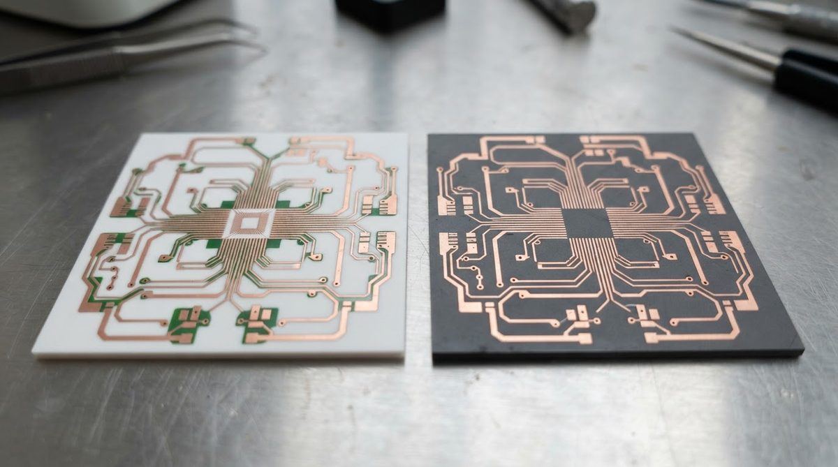
Suppose you are packaging a 1200 V / 50 A SiC MOSFET die (4.5 × 4.5 mm) with 120 W continuous dissipation. The design requires a 30 × 30 mm substrate, 0.32 mm DBC copper, AlN base, NiAu surface finish, and 200 µm minimum trace width.
- AlN substrate (30 × 30 × 0.635 mm): ~$3.00–$5.50 per piece at 5,000 pcs (based on published Maruwa and Kyocera distributor pricing).
- DBC metallization (0.32 mm Cu, both sides): ~$2.00–$4.00 per piece, including patterning and etching.
- NiAu plating: ~$0.80–$1.50 per piece.
- Laser scribing, inspection, packaging: ~$0.50–$1.00 per piece.
Estimated total: $6.30–$12.00 per substrate at 5,000 pieces. At 100-piece prototype quantity, multiply by roughly 3–4×. Switching from AlN to 96% alumina would save $2–$4 per piece but raises junction-to-case thermal resistance by approximately 0.15–0.25 °C/W for this die size, which may push junction temperature above the SiC die’s 175 °C rating under worst-case conditions.
Enter your own substrate dimensions, material, and quantity below to get a ballpark estimate for your semiconductor packaging PCB cost.
[pcb_calc type=”pcb-quote”]
How to Reduce Semiconductor Packaging PCB Cost
Right-size the material. If thermal simulation shows your junction temperature stays 20 °C below the limit on 96% alumina, do not specify AlN. This single decision can cut substrate cost by 60–80%.
Relax tolerances where the process allows. A 100 µm line/space design can use DBC or thick film. Dropping to 50 µm forces thin film or DPC, roughly doubling metallization cost. If your wire-bond pitch allows it, stay above 100 µm.
Panel utilization matters. Work with your supplier to fit the maximum number of units per panel. A 30 × 30 mm substrate fits 9-up on a 114.3 × 114.3 mm panel versus 4-up on a smaller standard. That difference alone can reduce per-piece cost by 15–25%. For a full breakdown of how panel size, tooling, and NRE charges affect pricing, see the ceramic PCB cost breakdown.
Consolidate surface finish. Electroless NiPdAu is often specified by default for wire bonding, but if your process uses solder-attach only, ENIG or even bare Cu with OSP may suffice at lower cost.
When a Ceramic Substrate Is Not the Right Choice
If your semiconductor package operates below 150 °C junction temperature, dissipates under 5 W, and does not require hermetic sealing, a metal-core PCB (MCPCB) or high-Tg FR-4 laminate will cost 80–95% less and meet the requirement. Standard BGA and QFN packages on organic substrates handle the vast majority of consumer and low-power industrial ICs. Ceramic substrates earn their cost in power semiconductors (SiC, GaN, IGBT), high-reliability environments (automotive under-hood, aerospace, downhole), and RF/MMIC packaging where dielectric loss and dimensional stability matter. If your application does not fall into one of these categories, the cost premium is hard to justify. Sensor and MEMS packaging is another area where ceramic substrates compete; see sensor ceramic substrate cost for that comparison.
Frequently Asked Questions
Is DBC or AMB cheaper for semiconductor packaging?
DBC is cheaper, typically 30–80% less than AMB for the same substrate size and copper thickness. AMB is necessary when bonding to AlN or Si₃N₄, or when copper thickness exceeds roughly 0.5 mm, because the active braze provides stronger adhesion than the Cu–O eutectic used in DBC.
How much does AlN cost compared to alumina for a typical power module substrate?
AlN substrates cost 3–5× more than 96% alumina per unit area at equivalent thickness and finish. For a 30 × 30 mm substrate at 5,000-piece volume, that translates to roughly $3–$5.50 for AlN versus $0.80–$1.50 for 96% Al₂O₃.
Can I use thick-film metallization for semiconductor die attach?
Yes, thick-film metallization works well for die attach when line/space requirements are above 100 µm and the operating frequency is below a few GHz. It is common in power module packaging and hybrid circuits. For fine-pitch flip-chip or MMIC applications, thin film is required.
What is the minimum order quantity for ceramic packaging substrates?
Most ceramic PCB suppliers accept prototype orders starting at 5–25 pieces, though per-piece cost at that volume is 3–5× higher than at production quantities of 5,000+. Tooling and NRE charges (typically $200–$800 for a new DBC pattern) also weigh more heavily at low volumes.
Do ceramic substrates need special handling during assembly?
Ceramic substrates are brittle and can crack under point loads or flexure. Use vacuum pick-and-place tooling rather than mechanical grippers. Store substrates in anti-static trays with edge support, and avoid stacking without separators. Soldering processes (reflow, vapor phase) are standard, but thermal ramp rates should stay under 3–4 °C/s to avoid thermal shock on thicker substrates.