Wire bonding is a solid-state welding process that uses a thin metal wire (typically 15–75 µm diameter) to create an electrical connection between a semiconductor die pad and a bond pad on a substrate or lead frame. Understanding this wire bonding definition matters because the process remains the dominant interconnect method in semiconductor packaging, accounting for over 90 % of all die-level connections worldwide, per SEMI industry estimates. For engineers evaluating ceramic substrates, wire bonding is often the assumed interconnect—and the substrate must be designed to support it.
Wire Bonding Definition and Core Mechanism
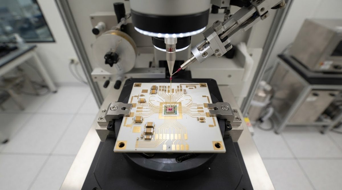
At its simplest, the wire bonding definition describes a process in which a bonding tool—called a capillary or wedge—presses a fine wire against a metallized pad while applying a combination of heat, pressure, and ultrasonic energy. The resulting intermetallic joint forms in milliseconds. The wire is then looped to a second pad and bonded again, completing one interconnect.
Two dominant techniques exist:
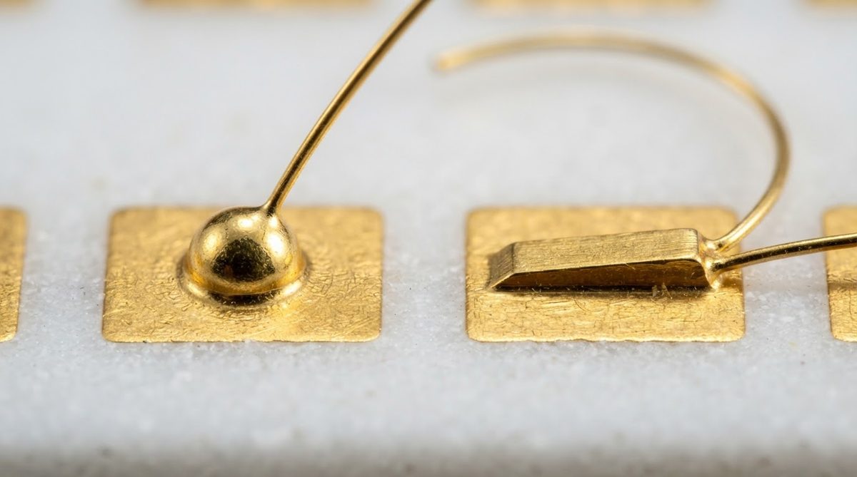
- Ball bonding — An electric flame-off (EFO) melts the wire tip into a ball. The ball is pressed onto the die pad (first bond), looped, then wedge-bonded to the substrate pad (second bond). Used almost exclusively with gold or copper wire. Typical speeds exceed 15 wires per second on modern bonders.
- Wedge bonding — The wire is pressed flat against the pad without forming a ball. Both first and second bonds are wedge-shaped. Preferred for aluminum wire and for applications requiring a low loop height. Slower than ball bonding but produces a smaller footprint.
Common Wire Materials
| Material | Typical Diameter | Primary Use | Note |
|---|---|---|---|
| Gold (Au) | 18–50 µm | Ball bonding, high-reliability | Excellent corrosion resistance; high cost |
| Copper (Cu) | 18–50 µm | Ball bonding, cost-sensitive | Harder than Au; requires forming gas to prevent oxidation |
| Aluminum (Al) | 25–500 µm | Wedge bonding, power devices | Large-diameter Al ribbon used in IGBT modules |
| Silver (Ag) | 18–50 µm | Ball bonding, LED packaging | Lower cost than Au with good conductivity |
Diameters are representative ranges; actual selection depends on current-carrying requirements and pad geometry.
Why Ceramic Substrates Suit Wire Bonding
The wire bonding definition implies a process that demands a rigid, dimensionally stable surface. Ceramic substrates—alumina (Al₂O₃), aluminum nitride (AlN), and silicon nitride (Si₃N₄)—meet that requirement better than organic laminates for several reasons:
- Flatness. Blank ceramic substrates hold surface flatness within a few micrometres, preventing bond-pad coplanarity issues that cause missed bonds.
- Thermal stability. Ceramics do not soften or outgas at the 150–220 °C stage temperatures used during thermosonic bonding.
- CTE match. Alumina’s CTE of ~7 ppm/°C is far closer to silicon (~3 ppm/°C) than FR-4 (~14–17 ppm/°C), reducing thermal-cycle stress on wire bonds.
Metallized ceramic substrates with gold or silver thick-film pads are the standard landing surface for wire bonds in hybrid microelectronics, power modules, and RF packages. Proper pad metallization is critical to achieving the intermetallic joint described in any wire bonding definition.
When Wire Bonding Is Not the Right Choice
Wire bonding adds height (loop heights of 75–250 µm are typical) and is inherently sequential—one wire at a time. For very high I/O counts (>1 000 connections per die) or ultra-thin packages, flip-chip solder bumps or copper-pillar interconnects are faster and more compact. Wire bonds also carry less current per connection than direct solder attach, making them less suitable for single-connection high-current paths above roughly 10 A without paralleled wires or ribbon bonding.
Frequently Asked Questions
What metals can be wire-bonded to a ceramic PCB?
Gold, aluminum, copper, and silver wires all bond successfully to ceramic substrates with matching pad metallization. Gold wire on gold thick-film pads is the most proven combination in high-reliability applications per MIL-STD-883 (Test Method 2011).
How strong is a wire bond?
A 25 µm gold ball bond typically pulls at 3–12 gf in a destructive pull test, depending on loop geometry and bonding parameters. MIL-STD-883 TM 2011 sets minimum pull-force criteria by wire diameter.
Can wire bonding be done on FR-4?
Yes, but it is uncommon. FR-4 is softer and less flat than ceramic, which makes consistent bonding harder. Chip-on-board (COB) assemblies on FR-4 exist for consumer products, but high-reliability designs almost always use ceramic or metal lead frames.
What is the difference between wire bonding and die attach?
Die attach fixes the semiconductor chip to the substrate (using solder, epoxy, or sintered silver). Wire bonding happens after die attach and creates the electrical connections from the chip’s pads to the substrate’s circuit traces. They are sequential steps in the same assembly flow, described further in overviews of ceramic PCB manufacturing.
Does the wire bonding definition change for ribbon bonding?
Ribbon bonding is a variant of wire bonding that uses a flat metal ribbon instead of round wire. The core wire bonding definition still applies—solid-state welding via heat, pressure, and ultrasonic energy—but ribbon bonds carry higher current per connection and are common in power semiconductor modules.