What Is Solder Mask Definition?
Solder mask definition refers to the method used to control the solderable area of a PCB pad. The two approaches — solder mask defined (SMD) and non-solder-mask defined (NSMD) — determine whether the mask opening or the copper etch sets the pad boundary. Choosing the correct solder mask definition affects solder joint reliability, inspection access, and pad adhesion, especially on ceramic substrates where thermal cycling stresses are severe.
Solder mask itself (also called solder resist) is a thin polymer or glass coating applied over the conductive traces of a PCB, leaving only designated pads, test points, and vias exposed. Its primary jobs are to prevent solder bridges during assembly, protect copper from oxidation, and provide electrical insulation between adjacent traces.
On organic boards (FR-4, polyimide), solder mask is almost always a liquid photoimageable (LPI) epoxy, typically 15–25 µm thick. On ceramic substrates, the situation differs. Many thick-film and thin-film ceramic PCBs use a glass-based overglaze or dielectric paste fired at 500–850 °C instead of an organic LPI, because standard epoxy solder masks cannot survive the operating temperatures ceramic boards are often chosen for.
SMD vs NSMD: How Solder Mask Definition Works
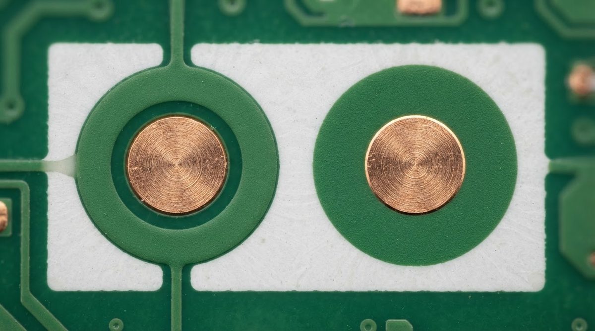
The two solder mask definition styles control the solderable pad area in opposite ways:
- SMD (Solder Mask Defined): The mask opening is smaller than the copper pad. The solder mask overlaps the pad edge, so the mask controls the solderable area. This improves pad adhesion to the base substrate and is common on ceramic boards where copper-to-ceramic bond strength matters.
- NSMD (Non-Solder Mask Defined): The mask opening is larger than the copper pad, exposing the full pad plus a small annular gap. The copper etch defines the solderable area. NSMD gives better solder joint inspection and a larger contact area between solder and copper, which generally produces more reliable BGA joints per IPC-7095.
For BGA pitches below 0.5 mm, NSMD is the standard recommendation because it allows self-centering during reflow. For large power pads on ceramic substrates operating above 200 °C, SMD can be preferable because the mask overlap mechanically anchors the pad against thermal cycling stress.
| Parameter | SMD (Solder Mask Defined) | NSMD (Non-Solder Mask Defined) |
|---|---|---|
| Pad area controlled by | Mask opening | Copper etch |
| Mask-to-pad relationship | Mask overlaps copper edge | Mask clears copper edge by 50–75 µm typical |
| Solder joint shape | Narrower at pad, wider at component | Barrel-shaped, full pad contact |
| Pad adhesion to substrate | Higher (mask anchors pad) | Lower (pad edge exposed) |
| Inspection access | Limited (pad edge hidden) | Full (pad perimeter visible) |
| Recommended for fine-pitch BGA (< 0.5 mm) | No | Yes (per IPC-7095) |
| Recommended for high-temp ceramic power pads | Yes | Case-by-case |
Solder Mask Definition on Ceramic PCBs
Many ceramic PCB designs omit solder mask entirely. Direct-bonded copper (DBC) and active metal brazed (AMB) substrates for power modules often rely on wide trace spacing (≥ 0.5 mm) and selective metallisation to prevent bridging, making a mask unnecessary. When a mask is required on a ceramic board, engineers typically specify a fired glass dielectric layer rather than an organic LPI. The glass layer withstands continuous operation above 300 °C and matches the low CTE of the ceramic, avoiding the cracking that would occur with an epoxy mask under thermal cycling.
When solder mask definition is needed on a ceramic substrate, SMD pads are the more common choice. The fired glass overglaze bonds well to both the metallisation and the alumina or aluminum nitride beneath it, reinforcing the pad against shear forces during thermal cycling. NSMD remains appropriate for ceramic boards carrying fine-pitch BGAs where self-centering and inspection access outweigh adhesion concerns.
Enter your pad size, mask opening, and pitch to see whether SMD or NSMD solder mask definition suits your layout and what clearance margins to target.
When Solder Mask May Not Be Needed
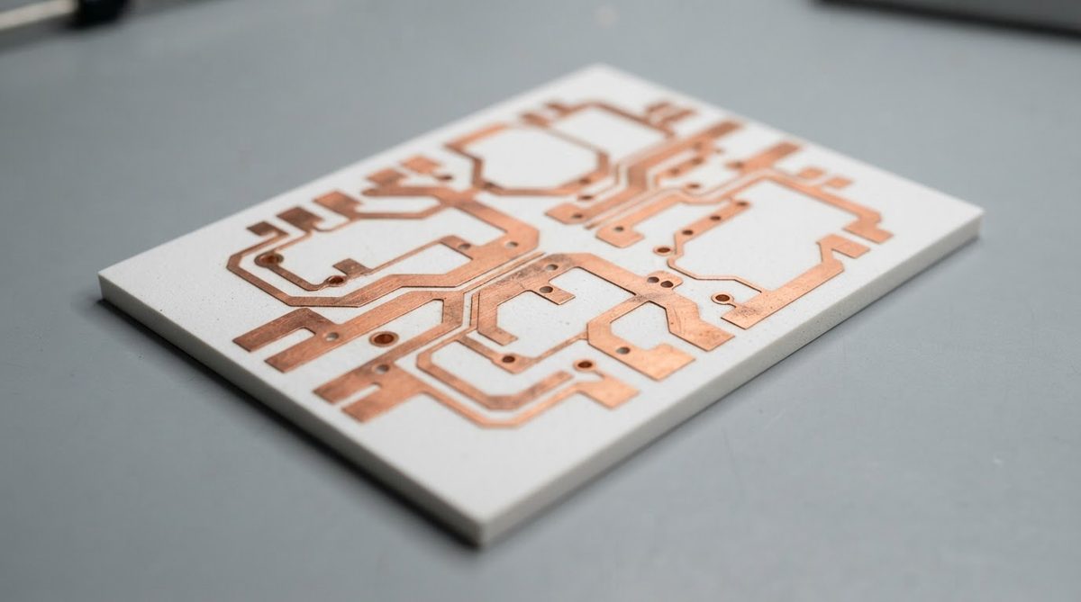
Solder mask adds cost and a process step. Skip it when trace spacing is wide enough to prevent bridging (generally > 0.4 mm for hand soldering, > 0.25 mm for automated reflow), when the board operates in a sealed environment where oxidation is not a concern, or when wire bonding is the primary interconnect method and no reflow soldering occurs. In these cases, the solder mask definition question becomes moot because there is no mask to define the pad.
Frequently Asked Questions
Does solder mask definition affect solder joint reliability?
Yes. NSMD solder mask definition generally produces more reliable BGA solder joints because the solder wets the full pad perimeter, creating a barrel-shaped joint with better fatigue life. SMD joints concentrate stress at the mask edge but offer stronger pad adhesion, which can matter more on ceramic substrates under severe thermal cycling.
Can I mix SMD and NSMD pads on the same board?
You can. It is common to use NSMD for fine-pitch BGAs and SMD for large thermal or power pads on the same ceramic PCB. Clearly document both solder mask definition types in your fabrication notes and Gerber files so the manufacturer applies the correct openings.
What solder mask material is used on ceramic PCBs?
Most ceramic PCBs that require a mask use a fired glass dielectric rather than the LPI epoxy common on FR-4. The glass is screen-printed and fired at 500–850 °C, producing a coating that survives continuous operation above 300 °C and closely matches the CTE of alumina or AlN substrates.
How do I specify solder mask definition in my Gerber files?
The solder mask Gerber layer defines the mask openings. For SMD pads, draw the mask opening smaller than the copper pad so the mask overlaps the pad edge. For NSMD pads, draw the mask opening 50–75 µm larger per side than the copper pad. Add a fabrication note stating which pads are SMD and which are NSMD to avoid ambiguity.