Thermal Resistance Definition
The thermal resistance definition used in electronics is straightforward: thermal resistance (Rth) is the temperature difference between two points divided by the heat power flowing between them, expressed in °C/W. A lower Rth means heat escapes more easily, keeping components cooler. The concept is analogous to electrical resistance in Ohm’s law — temperature replaces voltage, and heat flow replaces current. Understanding this thermal resistance definition is the first step toward sizing substrates, heat sinks, and thermal interface materials correctly.
The general formula is:
Rth = ΔT / P
- ΔT — temperature difference (°C) between the heat source and the reference point
- P — dissipated power (W)
For a solid slab of material, conduction thermal resistance is calculated as:
Rth = t / (k × A)
- t — thickness (m)
- k — thermal conductivity (W/m·K)
- A — cross-sectional area (m²)
Worked Example: Applying the Thermal Resistance Definition to Ceramic vs FR-4
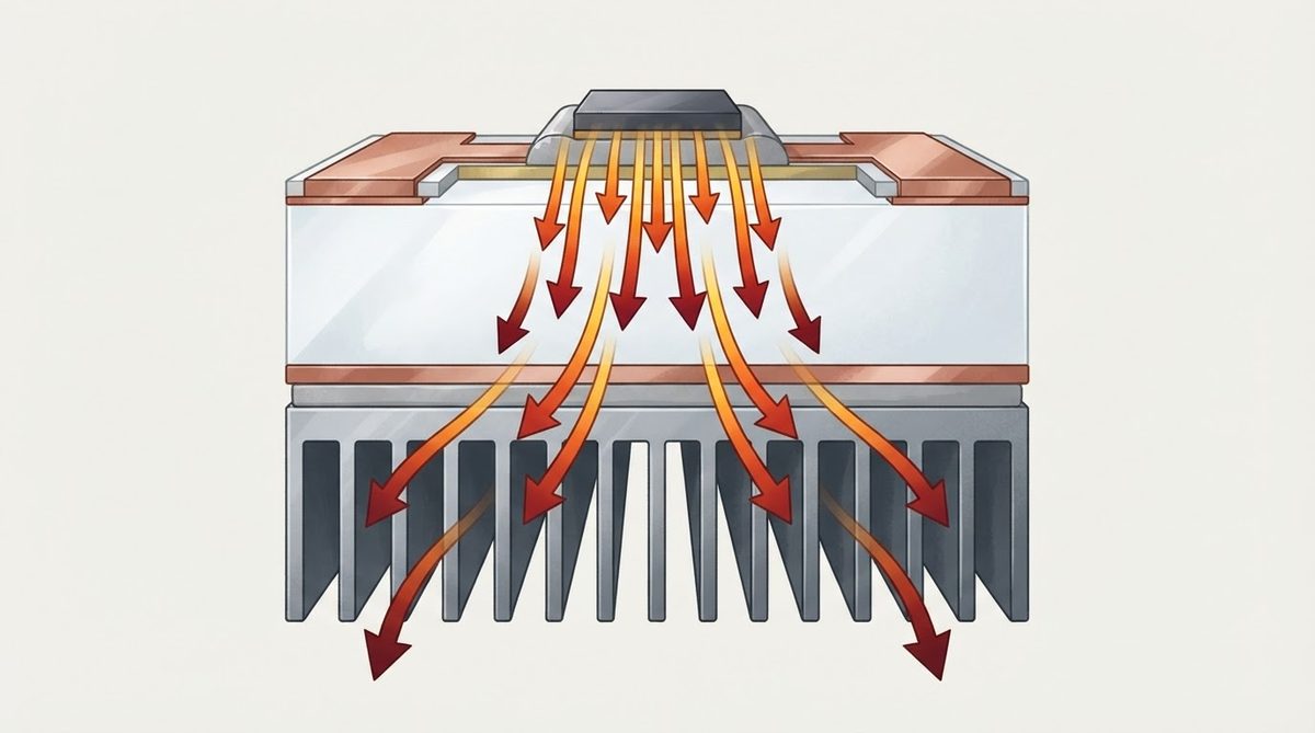
A 0.635 mm thick 96% alumina substrate (k ≈ 24–28 W/m·K per CoorsTek ADS-96R datasheet) under a 5 mm × 5 mm heat source gives roughly Rth = 0.000635 / (26 × 0.000025) ≈ 0.98 °C/W through the substrate alone. Replace that with FR-4 (k ≈ 0.3 W/m·K) at the same geometry and Rth jumps to about 85 °C/W — nearly two orders of magnitude worse. For a full worked calculation, see how to calculate thermal resistance of a ceramic PCB.
| Parameter | 96% Alumina | FR-4 | Unit | Source |
|---|---|---|---|---|
| Thermal conductivity (k) | 24–28 | 0.25–0.35 | W/m·K | CoorsTek ADS-96R / IPC-4101 |
| Substrate thickness | 0.635 | 0.635 | mm | — |
| Heat source area | 25 | 25 | mm² | — |
| Calculated Rth (substrate only) | ≈ 0.98 | ≈ 85 | °C/W | Rth = t / (k × A) |
Components of Junction-to-Ambient Thermal Resistance
In a real assembly, total Rth from junction to ambient (θJA) is a series chain of individual resistances. Each segment has its own thermal resistance, and the overall value is their sum:
| Segment | Symbol | What It Covers |
|---|---|---|
| Junction to case | θJC | Die, die attach, package |
| Case to board | θCB | Solder joint, pad interface |
| Board (substrate) | Rthsub | PCB dielectric layer |
| Board to heatsink | θBH | TIM, mounting interface |
| Heatsink to ambient | θHA | Convection and radiation |
Ceramic substrates primarily reduce Rthsub. Because alumina and aluminum nitride conduct heat 80–600× better than FR-4’s resin matrix, the substrate often drops from the dominant thermal resistance to a minor contributor in the chain.
Enter your component’s power dissipation, substrate properties, and package thermal data below to estimate junction temperature rise.
[pcb_calc type=”junction-temperature”]
Reducing Thermal Resistance with Vias
Thermal vias drilled beneath a heat source create parallel copper paths through the substrate, lowering the effective Rth. Each plated via acts as a low-resistance thermal shunt. On organic boards this technique is essential; on ceramic substrates it is less critical because the base material already conducts well, but it is still used under high-flux components where every fraction of a °C/W matters.
Use this calculator to size a thermal via array and compare the resulting thermal resistance with and without vias.
[pcb_calc type=”thermal-via”]
When Thermal Resistance Is Not Your Problem
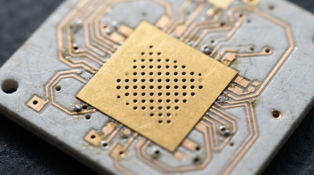
If your hottest component dissipates under 0.25 W and ambient stays below 50 °C, standard FR-4 with a copper pour is usually adequate. Switching to ceramic adds cost and lead time without meaningful benefit. Ceramic substrates earn their keep above roughly 1–2 W/cm² flux density, in high-ambient environments, or where dielectric breakdown voltage matters alongside thermal performance.
Frequently Asked Questions
Is the thermal resistance definition the same for ceramic and organic PCBs?
Yes. The thermal resistance definition — Rth = ΔT / P — applies identically regardless of substrate material. What changes is the thermal conductivity (k) value plugged into the conduction formula. Ceramic substrates simply produce a much lower Rth because their k values are orders of magnitude higher than organic resins.
What units is thermal resistance measured in?
Thermal resistance is measured in °C/W (degrees Celsius per watt) or equivalently K/W. Both units are numerically identical because a one-degree change is the same size on both scales. Component datasheets from manufacturers like Infineon and ON Semiconductor typically use °C/W.
Can I just add up all the Rth values in the thermal path?
For a simple one-dimensional heat path, yes — series thermal resistances add directly, just like series electrical resistors. In practice, lateral heat spreading means the effective area changes at each interface, so a pure series sum slightly overestimates the total Rth. Finite-element simulation gives more accurate results for complex geometries.
Does solder joint quality affect thermal resistance?
Significantly. Voids in the solder layer between a component and the substrate act as insulating gaps, increasing the case-to-board thermal resistance (θCB). Industry guidance per IPC-7095 recommends keeping void area below 25% under thermal pads to maintain the expected Rth value.
Related Terms
Thermal resistance values depend heavily on how metallization is applied. Thick-film and thin-film processes produce different interface qualities and layer thicknesses, both of which affect the overall Rth stack. Browse the full ceramic PCB terms reference for additional definitions.