Die Attach Definition
The die attach definition is straightforward: die attach is the assembly step in which a bare semiconductor die is permanently bonded to a substrate or package cavity. The bond must conduct heat away from the die, provide mechanical support, and—in many designs—carry electrical current. Die attach is sometimes called die bonding or chip bonding. Understanding the die attach definition is essential for anyone designing or sourcing power modules, RF packages, or LED assemblies.
Common Die-Attach Methods
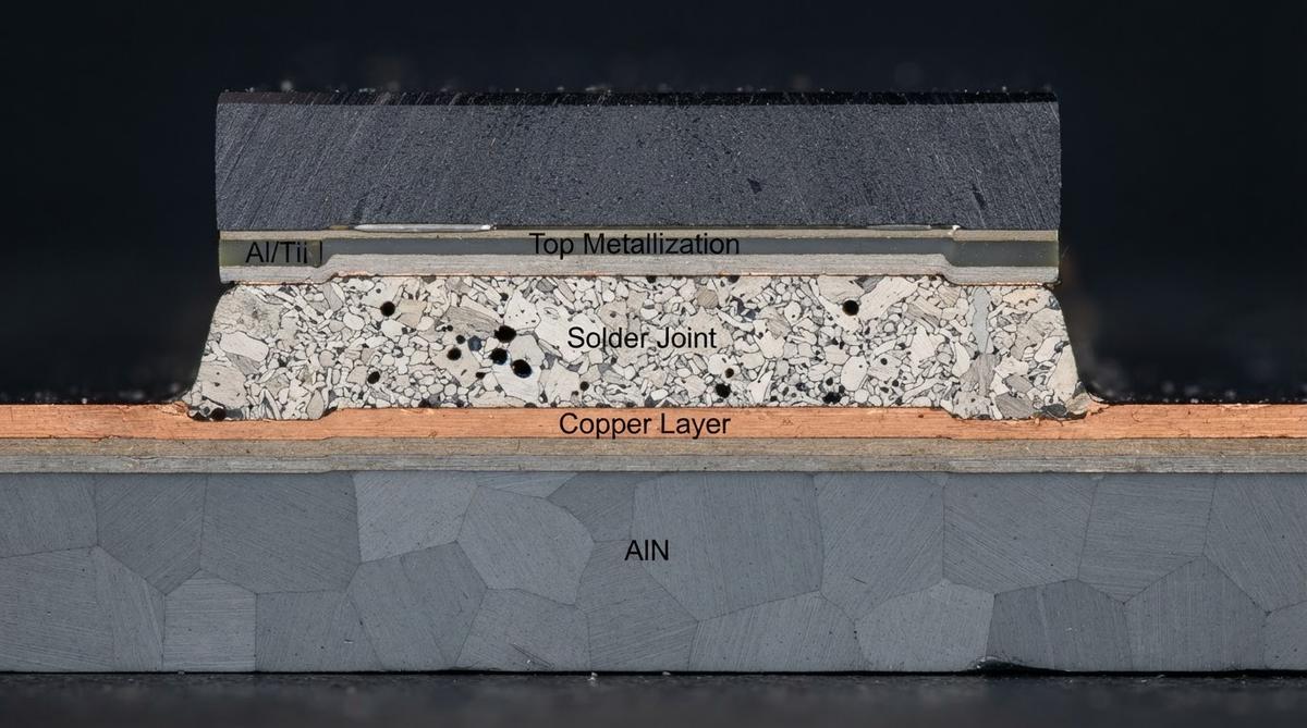
Several techniques fulfill the die attach function depending on power level, operating temperature, and reliability requirements:
- Solder die attach. A solder preform or paste (commonly AuSn, SnAgCu, or high-lead PbSn) is reflowed to form the bond. AuSn solder (80/20) reflows at roughly 280 °C and suits high-reliability applications per MIL-STD-883.
- Epoxy die attach. A silver-filled conductive epoxy is dispensed and cured at 150–175 °C. Lower cost, but higher thermal resistance than solder—typically 1–3 W/mK for the adhesive layer versus 50+ W/mK for AuSn solder.
- Sintered silver. A silver sintering paste is pressed and heated (200–250 °C, 10–30 MPa). The resulting bond layer can exceed 200 W/mK thermal conductivity and withstand junction temperatures above 250 °C, making it the preferred die attach method for SiC and GaN power devices.
- Eutectic die attach. A gold–silicon or gold–tin eutectic is formed directly between the die backside metallization and the substrate pad, without a separate preform. Requires precise temperature control and a well-prepared metallization surface.
Why Ceramic Substrates Suit Die Attach Applications
Ceramic substrates—Al₂O₃, AlN, and Si₃N₄—offer three advantages over organic boards for die attach. First, their CTE (6–7 ppm/°C for alumina, 4.5 ppm/°C for AlN) is closer to silicon (2.6 ppm/°C) and SiC (4.0 ppm/°C) than FR-4 (14–17 ppm/°C). A smaller CTE mismatch reduces shear stress on the bond line during thermal cycling, which directly improves the long-term reliability of the die attach joint. Second, ceramics tolerate the process temperatures of AuSn reflow and silver sintering without degradation. Third, ceramic surfaces accept robust pad metallizations—such as DPC copper or thick-film gold—that wet and bond reliably under solder or sinter processes.
When Ceramic Is Not Needed for Die Attach
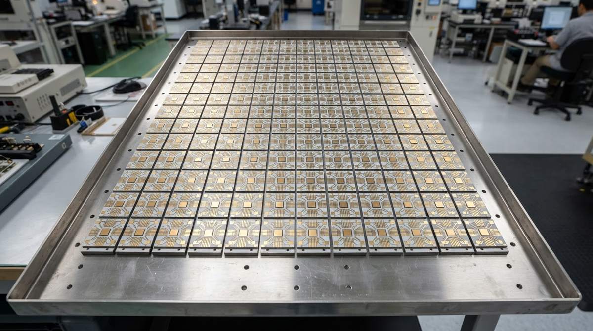
If the die dissipates under roughly 1 W and operates below 125 °C, epoxy die attach onto an FR-4 or metal-core PCB is usually sufficient and far cheaper. Ceramic substrates add cost and lead time that are hard to justify for low-power consumer electronics. In those cases the die attach definition still applies, but the substrate choice shifts to lower-cost organic materials.
FAQ
What is the difference between die attach and wire bonding?
Die attach bonds the bottom of the die to the substrate. Wire bonding connects the top-side pads of the die to the substrate traces. They are sequential steps: die attach comes first.
Can you die-attach directly to a bare ceramic surface?
No. The ceramic must have a metallized pad—typically gold, silver, or copper—to allow solder wetting or sinter bonding. Bare alumina or AlN will not form a reliable die attach bond with any standard material.
How thick is a typical die-attach layer?
Solder bond lines are usually 15–50 µm thick. Sintered silver layers are thinner, typically 15–30 µm. Epoxy layers range from 25–75 µm depending on dispensing method.