Ceramic PCB recycling is both technically feasible and often economically worthwhile: the metallization layers contain copper, silver, gold, or palladium worth recovering, while the ceramic substrate itself (Al₂O₃, AlN, Si₃N₄) is chemically inert and classified as non-hazardous solid waste in most jurisdictions. The challenge is separating those metals from a substrate that does not dissolve in standard acid baths the way FR-4 epoxy does.
Key Takeaways
- Copper, silver, and gold on ceramic substrates are recoverable through mechanical crushing followed by hydrometallurgical or pyrometallurgical processing.
- Bare alumina and aluminum nitride substrates are inert and non-toxic; they can be landfilled as construction-grade waste in most regions, though recycling is preferred.
- Beryllium oxide (BeO) ceramic boards require hazardous-waste handling — never crush, grind, or landfill them without specialist disposal. See the beryllium oxide safety guide for details.
- EU WEEE Directive (2012/19/EU) and US EPA regulations classify assembled ceramic PCBs as e-waste; bare substrates without components may be exempt.
- Precious metal recovery from thick-film ceramic boards can yield 50–200 g of silver per kilogram of paste, making ceramic PCB recycling economically viable at moderate volumes.
What Makes Ceramic PCB Recycling Different from FR-4?
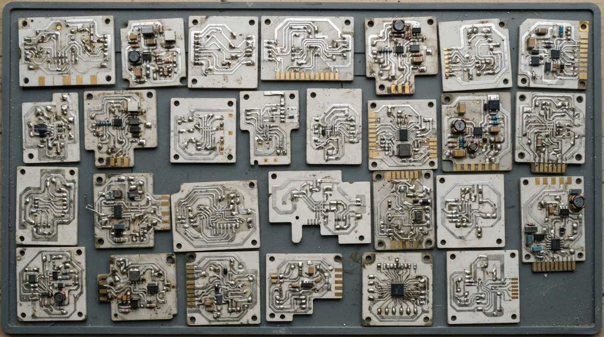
Standard FR-4 recycling relies on shredding the fiberglass-epoxy laminate and then using flotation, magnetic separation, or pyrolysis to isolate copper foil from the organic matrix. Ceramic boards have no organic matrix. The substrate is a fired oxide or nitride that does not burn, melt below ~1600 °C, or dissolve in common solvents. That inertness simplifies some steps and complicates others.
On the simpler side: ceramic substrates produce no brominated flame-retardant fumes during thermal processing, and no dioxin risk from incineration. On the harder side: mechanical separation is trickier because the metallization is bonded directly to the ceramic through processes like direct copper bonding or thin-film sputtering, not laminated with adhesive. You cannot peel the copper off.
Recoverable Materials and Their Value
The economic case for recycling ceramic PCBs depends almost entirely on the metallization, not the substrate. The table below lists typical recoverable metals by process type.
| Metallization Process | Primary Metals | Typical Loading | Recovery Method |
|---|---|---|---|
| Thick film (fired paste) | Silver, palladium, gold | 5–15 mg/cm² Ag; 0.5–3 mg/cm² Au | Acid leaching (HNO₃/HCl), electrolysis |
| DBC / AMB (direct bond copper) | Copper | 0.15–0.50 mm Cu foil | Mechanical crushing + gravity/eddy-current separation |
| Thin film (sputtered) | Gold, titanium, nickel, copper | 0.5–5 µm layers | Acid dissolution, selective precipitation |
| Plated finish (ENIG, ENEPIG) | Gold, nickel, palladium | 0.05–0.15 µm Au | Cyanide or thiosulfate leaching |
Typical values for commercially available metallized ceramics, for comparison only. Actual yields depend on board design and paste composition.
For DBC power modules, the copper layer alone can represent 30–50% of the board’s mass. At scrap copper prices around $8–9/kg (2024 LME average), a batch of 1,000 DBC substrates (25 × 25 mm, 0.3 mm Cu both sides) contains roughly 2.5–3 kg of recoverable copper. Not transformative revenue, but enough to offset processing costs.
Thick-film boards are more interesting financially. Silver-palladium pastes used in hybrid circuits can contain 50–200 g Ag per kilogram of paste. A single tray of scrap thick-film ceramic hybrids may hold more precious metal value than a pallet of FR-4 boards.
Step-by-Step: How Ceramic PCBs Are Recycled
- Component removal. SMD components, wire bonds, and solder are stripped by reflow desoldering or selective heating. Components go into standard e-waste streams.
- Sorting by substrate material. Alumina, aluminum nitride, and Si₃N₄ substrates are separated. BeO substrates are diverted to hazardous-waste processing immediately.
- Mechanical size reduction. Boards are jaw-crushed to 5–10 mm fragments. Ceramic fractures cleanly; metal layers delaminate partially during crushing.
- Physical separation. Eddy-current separators pull out copper fragments. Gravity tables or air classifiers separate lighter ceramic dust from heavier metal particles.
- Hydrometallurgical recovery. Metal-rich fractions are dissolved in aqua regia (Au, Pt, Pd) or dilute nitric acid (Ag, Cu). Metals are recovered by selective precipitation, cementation, or electrowinning.
- Ceramic residue handling. Cleaned ceramic powder is either landfilled as inert waste or repurposed as an abrasive filler, refractory aggregate, or feedstock for alumina reclamation.
Regulatory Requirements
Assembled ceramic PCBs fall under e-waste regulations in most markets. In the EU, the WEEE Directive (2012/19/EU) requires producer take-back. In the US, regulations vary by state; California’s SB-20 and the federal Resource Conservation and Recovery Act (RCRA) apply. Bare, unmetallized ceramic substrates are generally classified as inert solid waste and are exempt from hazardous-waste rules.
The critical exception is beryllium oxide. BeO dust is a confirmed human carcinogen (IARC Group 1). OSHA’s permissible exposure limit is 0.2 µg/m³ (8-hour TWA) per 29 CFR 1910.1024. Never crush, grind, or sand BeO substrates without engineering controls and a hazardous-waste manifest. Even intact BeO boards should be disposed of through a licensed beryllium waste handler.
Aluminum nitride is sometimes flagged as a concern, but the fired ceramic form is stable and non-toxic under normal handling. The AlN toxicity FAQ covers this in detail.
When NOT to Recycle Ceramic PCBs
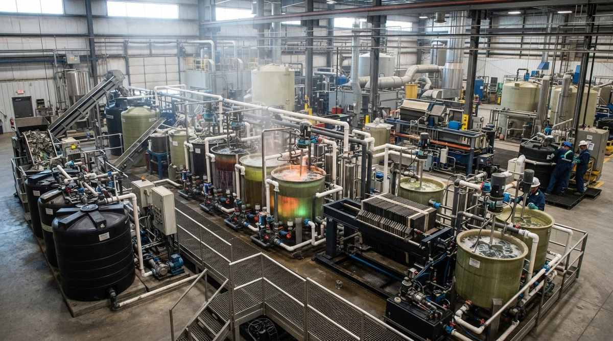
Recycling is not always the right call. Consider disposal or alternative handling in these cases:
- Low volume, low metallization. A handful of bare alumina test coupons with thin-film traces hold negligible metal value. Landfilling as inert waste is simpler and cheaper.
- BeO substrates without a licensed handler nearby. Shipping hazardous ceramic waste across borders adds cost and liability. Contact your regional EPA office or equivalent authority for approved facilities.
- Classified or ITAR-controlled assemblies. Defense electronics may require destruction-with-certification rather than recycling. Crushing and acid dissolution can satisfy destruction requirements, but the process must be documented.
- Contaminated boards. Substrates exposed to radioactive environments (medical isotope production, nuclear instrumentation) follow radioactive waste protocols, not standard e-waste streams.
Can the Ceramic Substrate Itself Be Reused?
In principle, yes. Alumina is thermally and chemically stable enough to survive metal stripping and re-metallization. In practice, the economics rarely work. Stripping metallization without micro-cracking the substrate is difficult, and the cost of inspection and re-qualification exceeds the cost of a new blank substrate. Some facilities grind recovered alumina into powder for use as a polishing abrasive or refractory filler, which is a lower-value but practical reuse path.
If you are working with 96% alumina substrates, the raw material cost is low enough that recycling the ceramic itself is hard to justify economically. Higher-value substrates like AlN or Si₃N₄ have more incentive for material recovery, but the processing is more complex.
FAQ
Are ceramic PCBs considered hazardous waste?
No, with one exception. Alumina, aluminum nitride, silicon nitride, and zirconia substrates are chemically inert and classified as non-hazardous solid waste. Beryllium oxide is the exception — it is regulated as hazardous due to carcinogenic dust risk and requires special handling under OSHA 29 CFR 1910.1024.
Can I throw away a few scrap ceramic boards in regular trash?
Bare, unmetallized ceramic substrates can generally go into regular waste as inert material. Metallized or assembled boards should go through e-waste channels because of the metals and solder (which may contain lead). Check your local regulations — some jurisdictions classify all PCBs as e-waste regardless of substrate material.
How much gold or silver can I recover from a ceramic PCB?
It depends on the metallization process. Thick-film hybrid circuits with silver-palladium paste are the richest source, yielding 50–200 g of silver per kilogram of paste. Thin-film or ENIG-finished boards contain far less — typically under 0.15 µm of gold, which is measurable but only economical to recover in large batches.
Do recyclers accept small quantities of ceramic PCBs?
Most precious-metal refiners accept ceramic PCB scrap by weight, with minimums around 1–5 kg. For smaller quantities, accumulate scrap in a labeled container and submit periodically. Some refiners offer lot-based assay and settlement, paying based on the actual metal content determined after processing.
Is aluminum nitride safe to grind for recycling?
Fired AlN ceramic is stable and non-toxic in solid form. Grinding produces fine dust that is an inhalation irritant, as with any ceramic powder, so standard respiratory protection (N95 or better) is appropriate. AlN dust can hydrolyze slowly in moist air to release trace ammonia, but this is a nuisance-level concern, not a toxicity hazard. Full details are in the ceramic PCB FAQ.
Next Step
If you are designing a ceramic board and want to plan for end-of-life from the start, consider metallization choices that simplify future recycling — DBC copper is easier and cheaper to recover than multi-layer thin-film stacks. For help specifying a board that balances performance with lifecycle cost, request a quote from our engineering team.