Blog
-
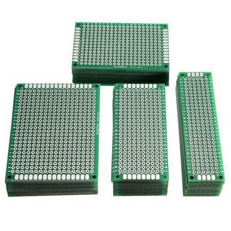
How much does a PCB prototype Cost?
Posted by
–
 Read more: How much does a PCB prototype Cost?
Factors Affecting PCB Prototype Cost 1. Board Size and Complexity The size and complexity of your PCB design significantly impact the overall prototype cost. Larger boards require more materials and take longer to manufacture, resulting in higher costs. Additionally, complex designs with intricate routing, multiple layers, and high component density […]
-
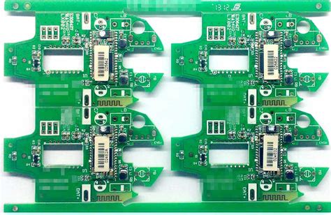 Read more: How to Choose the best PCB Prototype Service for Your New Product Introduction (NPI)?
Introduction When introducing a new product, choosing the right PCB Prototype Service is crucial for success. A reliable and experienced PCB prototype service can help you bring your product to market faster, with better quality and at a lower cost. In this article, we will discuss the key factors to […]
-
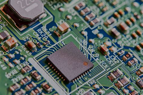 Read more: Have You Found Perfect China PCB Manufacturing House Service?
Introduction to PCB Manufacturing in China China has emerged as a global hub for PCB manufacturing, offering a wide range of services to meet the growing demand for printed circuit boards. With its advanced technology, skilled workforce, and cost-effective solutions, China has become a preferred destination for businesses seeking high-quality […]
-
Regal TP and MAP control circuit diagram
Posted by
–
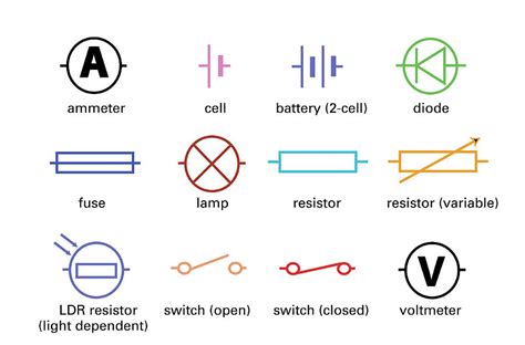 Read more: Regal TP and MAP control circuit diagram
Introduction to Regal TP and MAP Control Regal TP (Throttle Position) and MAP (Manifold Absolute Pressure) control is a crucial aspect of modern engine management systems. The
-
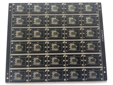 Read more: How to choose the PCB Prototype Manufacturer for critical electronic device design?
Understanding the Importance of Choosing the Right PCB Prototype Manufacturer The choice of a PCB Prototype Manufacturer can make or break your electronic device design project. A reliable and experienced manufacturer can provide you with high-quality prototypes that meet your specifications, while a subpar manufacturer can lead to delays, design […]
-
 Read more: Why you need to Optimize Bill of Materials for Rapid PCB Prototyping?
Introduction to PCB Prototyping and Bill of Materials PCB (Printed Circuit Board) prototyping is an essential step in the electronics design process. It allows designers to test and validate their designs before moving into mass production. Rapid PCB prototyping has become increasingly important as the demand for faster time-to-market and […]
-
The Favorable Factors of Shenzhen PCB
Posted by
–
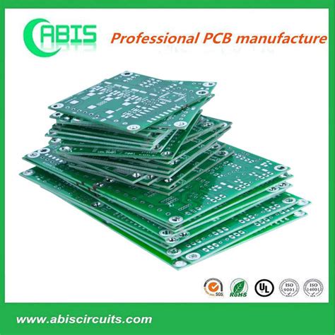 Read more: The Favorable Factors of Shenzhen PCB
Introduction to Shenzhen PCB Shenzhen, a city located in the southern part of China, has become a global hub for the production of printed circuit boards (PCBs). The city’s reputation for high-quality and cost-effective PCB manufacturing has made it a popular choice for businesses worldwide. In this article, we will […]
-
 Read more: Phones components top Vietnam s export value in Q
Vietnam’s Electronics exports Soar According to data from Vietnam’s General Statistics Office, the country’s total export value in the first quarter of 2023 reached $88.58 billion, a 12.4% increase compared to the same period in 2022. Among the various export categories, electronics exports stood out as a significant contributor to […]
-
12 cells Lipo Monitor and Balancer
Posted by
–
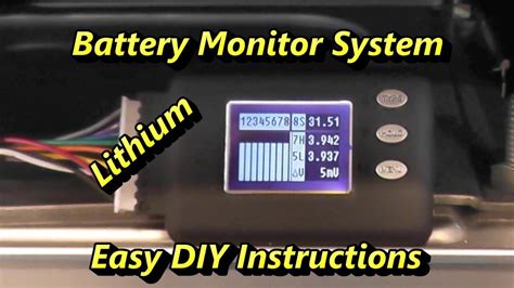 Read more: 12 cells Lipo Monitor and Balancer
Introduction to Lipo Monitors Lithium Polymer (LiPo) batteries have revolutionized the world of remote-controlled vehicles, such as drones, cars, and boats. These batteries offer high energy density, allowing for longer run times and more powerful performance. However, LiPo batteries require careful monitoring and balancing to ensure optimal performance and longevity. […]
-
Regal ABS serial data circuit diagram and table
Posted by
–
 Read more: Regal ABS serial data circuit diagram and table
Introduction to Regal ABS Regal ABS (Anti-lock Braking System) is a critical safety feature found in modern vehicles. It helps prevent the wheels from locking up during sudden braking, maintaining traction and steering control. The Regal ABS system relies on a complex network of sensors, controllers, and actuators to function […]


