Blog
-
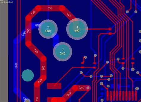
What are the telecom PCB design considerations?
Posted by
–
Read more: What are the telecom PCB design considerations?Introduction to Telecom PCB Design Telecom PCB design is a critical aspect of modern telecommunications systems. Printed Circuit Boards (PCBs) are the backbone of electronic devices, providing the necessary interconnections and support for various components. In the telecom industry, PCBs play a vital role in enabling reliable and efficient communication […]
-
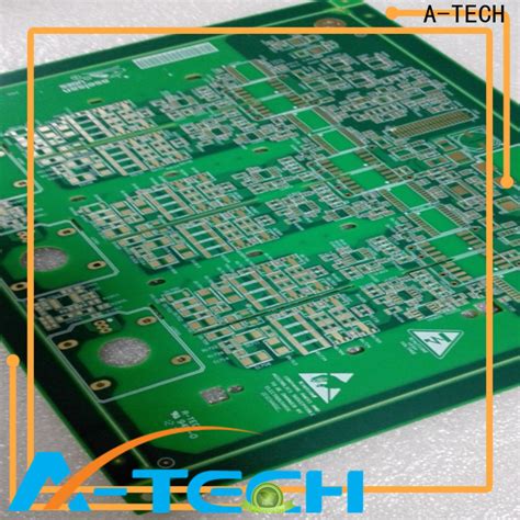 Read more: What are the top advantages of ordering bulk PCB assemblies?
Cost Savings One of the most significant advantages of ordering bulk PCB assemblies is cost savings. When you order PCBs in large quantities, you can take advantage of economies of scale, which means that the cost per unit decreases as the quantity increases. This is because the fixed costs associated […]
-
 Read more: What are the value added srices Tchnotronixn ofer?
Software Development Services Tchnotronixn offers comprehensive software development services that cover the entire software development lifecycle. Their team of experienced developers can help you create custom software solutions that meet your specific business requirements. Custom Software Development Tchnotronixn’s custom software development services include: Web application development Mobile application development Desktop […]
-
 Read more: What files/docs do you need for bare boards, PCB assembly and
Introduction to PCB documentation Printed Circuit Board (PCB) documentation is a crucial aspect of the PCB manufacturing process. It ensures that all the necessary information is available for the fabrication, assembly, and testing of the PCB. Proper documentation helps to minimize errors, reduce costs, and improve the overall quality of […]
-
 Read more: 7 Tips to Prepare Printed Circuit Board Assembly Documentation
Introduction Preparing comprehensive and accurate documentation is a critical step in the printed circuit board (PCB) assembly process. PCB documentation serves as a roadmap for the manufacturing team, guiding them through the assembly process and ensuring that the final product meets the required specifications. In this article, we will discuss […]
-
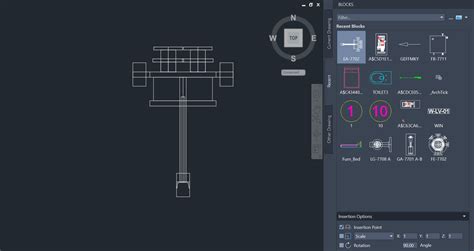 Read more: DownStream Releases Updated Versions of CAM350, DFMStream & BluePrint-PCB
CAD Software Giant Unveils Exciting New Features and Enhancements in Latest Release Downstream Technologies, a leading provider of PCB post-processing solutions, has recently announced the release of updated versions of their flagship products: CAM350, DFMStream, and BluePrint-PCB. These powerful tools are designed to streamline the PCB design process, improve manufacturing […]
-
What is a Heat Sink Printed Circuit Board and its importance in the electrical industry?
Posted by
–
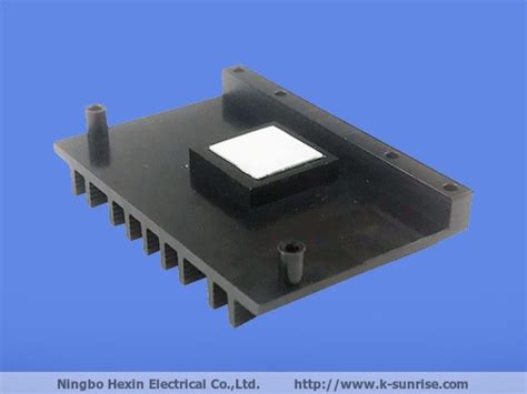 Read more: What is a Heat Sink Printed Circuit Board and its importance in the electrical industry?
Introduction to Heat Sink PCBs In the world of electronics, heat management is a crucial factor in ensuring the optimal performance and longevity of devices. As electronic components become more compact and powerful, the need for efficient heat dissipation solutions has become increasingly important. This is where Heat Sink Printed […]
-
 Read more: What is electromechanical assembly? What are the factors to consider for designing it?
What is Electromechanical Assembly? Electromechanical assembly refers to the process of combining electrical and mechanical components to create a functional system. This process involves the integration of various elements, such as printed circuit boards (PCBs), sensors, actuators, motors, and mechanical structures. The goal of electromechanical assembly is to ensure that […]
-
What is PCB assembly service?
Posted by
–
 Read more: What is PCB assembly service?
The Importance of PCB assembly in Electronics Manufacturing PCB assembly plays a vital role in the production of electronic devices across various industries, including: Consumer electronics Automotive Aerospace Medical devices Industrial equipment Telecommunications Without proper PCB assembly, electronic devices would not function as intended, leading to malfunctions, short lifespans, and […]
-
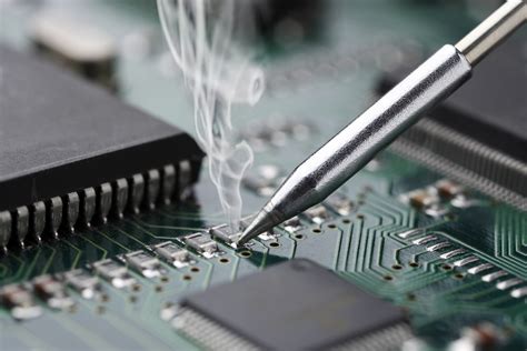
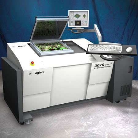 Read more: PCB Assembly Service Providers with In-Circuit Testing (ICT)
What is In-Circuit Testing (ICT)? In-Circuit Testing (ICT) is an automated testing method that verifies the functionality of individual components on a PCB by directly probing their connections. ICT is performed using specialized equipment called an ICT fixture, which consists of a bed of nails that makes contact with specific […]


