Blog
-
Read more: Top Factors to Consider while Choosing Large PCB Prototypes Manufacturing Service!
Understanding PCB Prototypes Before delving into the factors to consider, let’s first understand what PCB prototypes are and why they are essential in the electronics industry. What are PCB Prototypes? PCB prototypes, or printed circuit board prototypes, are initial versions of a PCB design that are used for testing and validation purposes before mass production.…
-
 Read more: Top Myths and Facts about PCB Prototyping and Assembly
Introduction to PCB Prototyping PCB prototyping is an essential step in the development of electronic devices. It involves creating a physical representation of a printed circuit board (PCB) design to test its functionality, compatibility, and performance before mass production. In this article, we will explore the top myths and facts about PCB prototyping and assembly…
-
 Read more: What Is Tenting Via & How It Plays Important Role In PCB Fabrication?
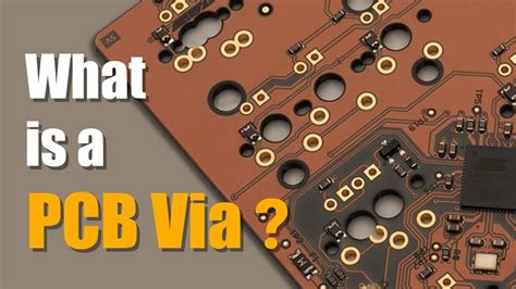
Introduction to Tenting Via In the world of printed circuit board (PCB) fabrication, tenting via is a crucial technique that plays a significant role in ensuring the reliability and functionality of the final product. Vias are small holes drilled through the layers of a PCB to create electrical connections between different layers. Tenting via is…
-
 Read more: Tenting Via – The Ultimate Guide To The Importance of PCBs
What is PCB Tenting? PCB Tenting, also known as Via Tenting or Tenting Vias, is a process used in the manufacturing of printed circuit boards (PCBs) where the vias (the small holes that allow electrical connections between layers of the PCB) are covered with a thin layer of solder mask material. This process is crucial…
-
 Read more: What is the Importance of HALT and HASS Test Methodologies for Telecom PCB Assemblies?
Introduction to HALT-HASS Testing In the highly competitive and rapidly evolving telecommunications industry, ensuring the reliability and durability of printed circuit board (PCB) assemblies is of utmost importance. Telecom equipment is expected to operate reliably under various environmental conditions and withstand the rigors of long-term use. To meet these challenges, manufacturers rely on advanced testing…
-
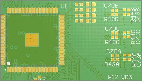
 Read more: What is the importance of PCB trace width in PCB design?
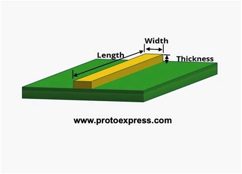
Understanding PCB trace width PCB trace width is a crucial aspect of printed circuit board (PCB) design that significantly impacts the overall performance, reliability, and manufacturability of the board. The width of a PCB trace refers to the physical dimension of the conductive copper pathways that carry electrical signals between components on the board. Properly…
-
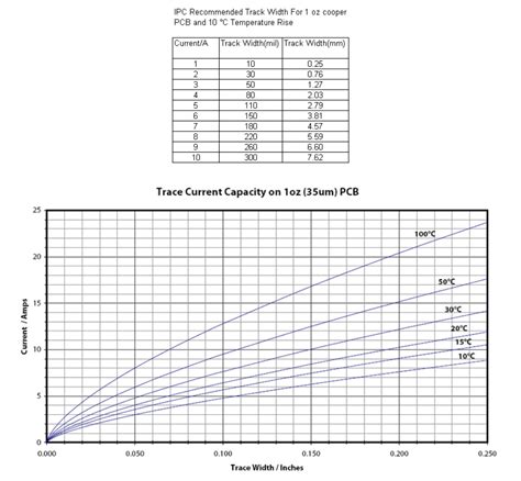
How to Determine PCB Trace Width and Current
Posted by
–
 Read more: How to Determine PCB Trace Width and Current
Understanding PCB trace width and Current Capacity When designing a printed circuit board (PCB), one of the crucial aspects to consider is the trace width and its current-carrying capacity. PCB traces are the copper paths that carry electrical signals and power between components on the board. Determining the appropriate trace width is essential to ensure…
-
Top 10 Best PCB routing practices!
Posted by
–
 Read more: Top 10 Best PCB routing practices!
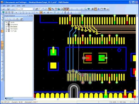
1. Keep Traces as Short and Direct as Possible One of the most fundamental PCB routing practices is to keep traces short and direct. This minimizes inductance, capacitance, interference, and signal integrity issues. Avoid meandering traces or routing at odd angles. Route high-speed signals first using the most direct path. Then route lower priority traces…
-
 Read more: What is the Importance of Thermal Pads in Circuit Board Manufacturing?
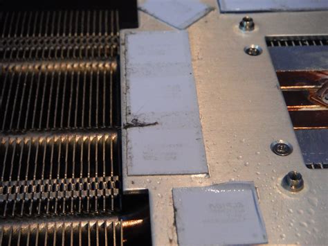
What are Thermal Pads? Thermal pads, also known as thermal interface materials (TIMs), are specialized materials designed to facilitate efficient heat transfer between electronic components and heat sinks or other cooling solutions. They are typically made from materials with high thermal conductivity, such as silicone, graphite, or ceramic-filled composites. Thermal pads are available in various…
-
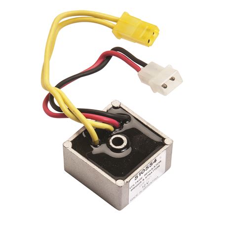 Read more: High Current Voltage Regulator: The Definitive Guide
What is a Voltage Regulator? A voltage regulator is an electronic device or circuit that maintains a constant voltage level in an electrical system, regardless of changes in load current or input voltage. Its primary function is to provide a stable and reliable power supply for various electronic devices and components. Voltage regulators are essential…


