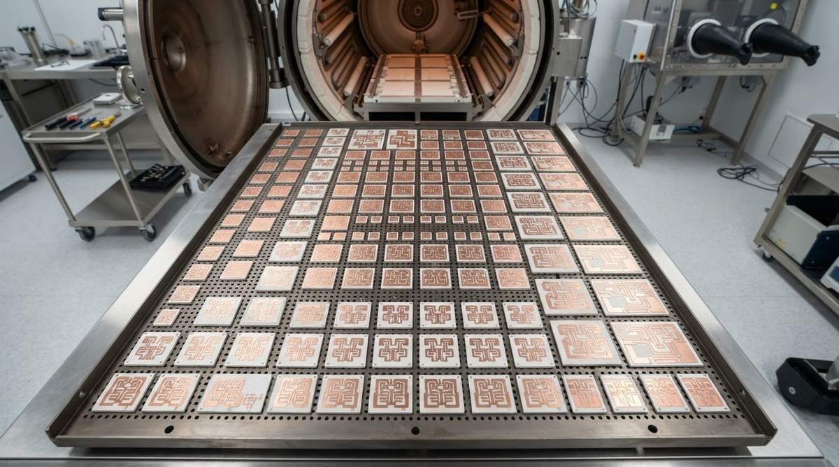
Active metal brazing (AMB) bonds copper foil (typically 300–800 µm) to a ceramic substrate using a titanium- or zirconium-bearing solder alloy fired at 800–900 °C in vacuum. Understanding AMB active metal brazing design rules matters because the braze layer, the thick copper, and the ceramic all interact under thermal cycling. Getting the geometry wrong leads to delamination, ceramic cracking, or premature solder-joint fatigue in the power module above. The rules differ substantially from those of DBC or thin-film processes, and this guide covers the critical ones.
Key Takeaways
- AMB supports copper thicknesses from 127 µm to 800 µm on a single substrate face—roughly 2–3× thicker than standard DBC.
- Minimum trace width is typically 0.3–0.5 mm; minimum gap between copper pads is 0.4–0.6 mm, depending on copper thickness and etch method.
- Si₃N₄ (silicon nitride) is the preferred AMB substrate for high-reliability power modules because its flexural strength (600–900 MPa per ASTM C1161) resists crack propagation under thermal cycling far better than Al₂O₃ or AlN.
- The braze alloy (commonly AgCu-Ti) wets the ceramic chemically, so no prior ceramic metallization step is needed—unlike thick-film or thin-film routes.
- Thermal-cycle life depends heavily on copper-edge geometry: a dimpled or etched-back copper edge reduces peak stress at the braze-ceramic interface by 30–50 % (per Fraunhofer IISB studies).
How AMB Differs from DBC
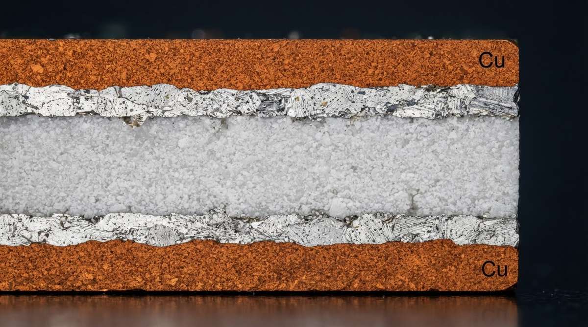
Both AMB and DBC (direct bonded copper) attach copper to ceramic, but the bonding mechanism and resulting design envelope differ. DBC relies on a CuO eutectic at ~1065 °C, which limits practical copper thickness to about 300 µm before residual stress causes ceramic fracture. AMB uses a reactive braze alloy at a lower temperature, accommodating thicker copper and stronger ceramics.
| Parameter | AMB | DBC | Unit | Notes |
|---|---|---|---|---|
| Bond temperature | 800–900 | 1 065–1 085 | °C | Vacuum vs. N₂ atmosphere |
| Max copper thickness | 800 | 300 | µm | Single side |
| Preferred ceramic | Si₃N₄, AlN, Al₂O₃ | Al₂O₃, AlN | — | Si₃N₄ rarely used with DBC |
| Min trace width | 0.3–0.5 | 0.3–0.5 | mm | Depends on Cu thickness |
| Min trace gap | 0.4–0.6 | 0.3–0.5 | mm | AMB wider gap for thicker Cu |
| Thermal-cycle life (−40/+150 °C) | >3 000 (Si₃N₄) | ~800–1 500 (Al₂O₃) | cycles | Per Infineon AN on power modules |
| Typical braze/bond layer thickness | 5–15 | <5 | µm | AgCuTi vs. CuO eutectic |
Typical values for commercially available material, for comparison only. Confirm against the datasheet for your specific grade.
Substrate Selection Under AMB Active Metal Brazing Design Rules
The ceramic you choose constrains almost every other design rule. Three substrates dominate AMB production:
Si₃N₄ (silicon nitride, 0.32 mm typical): Flexural strength of 600–900 MPa (per CoorsTek SN-88 datasheet) and fracture toughness of 6–7 MPa·√m make it the default for automotive-grade SiC and GaN power modules. Thermal conductivity is 70–90 W/mK—lower than AlN, but the thinner substrate partially compensates in total thermal resistance.
AlN (aluminum nitride, 0.635 mm typical): Thermal conductivity of 170–200 W/mK at 20 °C (per Maruwa HA-200 datasheet) is the highest among practical AMB ceramics. Flexural strength is only 300–400 MPa, so it cracks more readily under thick-copper stress. Best for applications where thermal performance outranks cycle life.
Al₂O₃ 96 % (alumina, 0.635 mm typical): Lowest cost, adequate for moderate-power designs. Thermal conductivity of 24–28 W/mK limits heat extraction. Flexural strength around 350 MPa. Used in industrial drives and lower-reliability tiers.
Critical AMB Active Metal Brazing Design Rules for Copper Geometry
Trace and Gap Dimensions
Minimum trace width scales with copper thickness. At 300 µm Cu, 0.3 mm traces are achievable with chemical etching. At 800 µm Cu, expect 0.5 mm minimum trace and 0.6 mm minimum gap. Etch factor (undercut per side ≈ 0.8–1.0× Cu thickness) must be included in your Gerber artwork. If your layout requires finer features, consider a DPC (direct plated copper) process instead, which reaches 20–50 µm lines but at much lower current capacity.
Copper-Edge Stress Relief
The single most common AMB failure mode is ceramic cracking originating at the copper pad edge. The CTE mismatch between copper (16.5 ppm/K) and Si₃N₄ (2.7 ppm/K) concentrates tensile stress in the ceramic directly beneath the copper perimeter during cooling. Two design countermeasures are standard:
- Edge dimpling (chemical etching): The copper edge is etched to a tapered or concave profile, reducing the stress singularity. Specify a dimple depth of 50–100 µm on your drawing.
- Ceramic overhang: Leave at least 0.8–1.5 mm of bare ceramic between the outermost copper edge and the substrate edge. This prevents edge-initiated cracks. Some designs use 2.0 mm for automotive qualification.
Backside Copper Balancing
An AMB substrate with copper on one side only will bow during cool-down from brazing temperature. The standard practice is to braze a copper layer of equal or near-equal thickness on the back side. If the back copper is patterned differently from the front, match the total copper area within 10–15 % to keep bow below 50 µm across a 50 × 50 mm substrate. This balancing rule is one of the most overlooked AMB active metal brazing design rules in early layout reviews.
Via and Through-Hole Rules
AMB substrates are almost always single-layer, with no plated through-holes. Electrical connections between top and bottom copper planes are made with edge castellations or wire bonds, not vias. If your design requires vertical interconnects through the ceramic, via filling in co-fired ceramics (HTCC or LTCC) is the appropriate process—AMB is not designed for it.
Enter your substrate dimensions, copper thickness, and dissipated power below to estimate junction-to-case temperature rise for your AMB stack.
Worked Example: Thermal Resistance of an AMB Stack
Consider a 40 × 40 mm Si₃N₄ AMB substrate, 0.32 mm ceramic, 0.3 mm Cu top, 0.3 mm Cu bottom, with a 10 × 10 mm SiC die dissipating 200 W.
- Copper top layer: Rth = t / (k × A) = 0.0003 m / (385 W/mK × 0.0001 m²) = 0.0078 K/W
- Si₃N₄ ceramic: Rth = 0.00032 / (80 × 0.0001) = 0.040 K/W (assuming 80 W/mK grade, heat spreading neglected for simplicity)
- Copper bottom layer: 0.0078 K/W (same as top)
- Total stack Rth ≈ 0.056 K/W
- ΔT across substrate at 200 W: 200 × 0.056 = 11.2 °C
This is a one-dimensional estimate. In practice, lateral heat spreading in the thick copper reduces the effective Rth by 20–40 %, and the solder or sinter layer between die and substrate adds 0.01–0.03 K/W. Use FEA for final validation.
When NOT to Use AMB
Fine-pitch signal routing: If your design needs traces below 0.2 mm or multi-layer interconnects, AMB is the wrong process. Use thin-film ceramic PCBs or LTCC instead.
Low-power or cost-sensitive applications: AMB substrates cost 3–10× more than DBC on alumina. If thermal-cycle requirements are modest (fewer than 1 000 cycles at −40/+125 °C), DBC on Al₂O₃ or AlN may be sufficient.
High-frequency RF circuits: AMB copper is too thick for controlled-impedance microstrip or stripline. Thin-film on alumina or AlN is the standard for RF above a few GHz.
Prototyping with fast turns: AMB requires vacuum brazing furnaces and long lead times (typically 4–8 weeks). If you need boards in days, DPC on alumina is faster to iterate.
FAQ
Can I use AMB with zirconia (ZrO₂) substrates?
No. Zirconia’s high CTE (~10 ppm/K) and phase-transformation behavior make it unsuitable for the thermal-cycling demands of power modules. Si₃N₄, AlN, and Al₂O₃ are the only ceramics used in production AMB.
What surface finishes can be applied to AMB copper?
Standard finishes include electroless nickel / immersion gold (ENIG), electrolytic Ni/Au, and bare copper with OSP. For die-attach by silver sintering, a thin Ag plating (3–8 µm) over Ni barrier is common. The finish choice depends on your die-attach and wire-bond process.
Does the braze alloy affect electrical isolation?
Yes. The AgCuTi braze is electrically conductive. Isolation between copper pads depends entirely on the gap width and the ceramic beneath it. For 3.0 kV isolation, a minimum gap of 1.0–1.5 mm is typical on 0.32 mm Si₃N₄, per IEC 60664-1 creepage and clearance tables. Verify with your specific voltage and pollution degree.
How flat does an AMB substrate need to be?
Bow and warp should be below 50 µm over a 50 × 50 mm substrate for reliable die attach. Achieving this requires balanced copper on both sides and controlled brazing profiles. Lapping the copper surface post-braze can further improve flatness to under 25 µm if needed for large-area sinter attach.
Is AMB compatible with aluminum wire bonding?
Yes. Aluminum wedge bonding directly to the AMB copper surface (with or without Ni plating) is the standard interconnect method in automotive power modules. Bond-pull strength on 300 µm bare Cu typically exceeds 1.5 N for 300 µm Al wire, meeting AQG 324 requirements.
Next Step
If your power-module design needs thick copper on ceramic, start by defining your substrate material, copper thickness, and isolation voltage. These three parameters lock in most of the remaining AMB active metal brazing design rules. For a design review or quote on AMB substrates, request a quote from AluminaPCB with your layout files and thermal requirements.
Last reviewed: 2025-07.